Semiconductor laser device and method of producing the same

a laser device and semiconductor technology, applied in semiconductor lasers, laser optical resonator construction, laser details, etc., can solve the problems of insufficient capacity of conventional semiconductor laser devices, catastrophic optical damage (cod), etc., to reduce the driving current in high-power operation, suppress the deterioration of crystallinity in the active layer, and reduce the diffusion of impurity atoms having second conductivity into the active layer.

Inactive Publication Date: 2008-09-30
SHARP KK
View PDF8 Cites 2 Cited by
  • Summary
  • Abstract
  • Description
  • Claims
  • Application Information

AI Technical Summary

Benefits of technology

[0023]It is an object of the invention to provide a semiconductor laser device having a reduced driving current at high-power operation and superior long-term reliability, and a method of producing the same.

Problems solved by technology

Further, one of factors that restrict increase in power of a semiconductor laser is catastrophic optical damage (COD), which tends to occur with increase of the optical power density in regions of an active layer in proximity of end faces of a laser cavity.
However, the conventional semiconductor laser devices have the following problems.
However, in the conventional semiconductor laser device in which the diffusion of impurity atoms into the active layer is suppressed, mere provision of a strain in the p-type cladding layer 6 does not make it possible to sufficiently suppress diffusion of p-type conductivity impurity atoms (Zn atoms) contained in the p-type cladding layer 6 into the active layer 4.
In the semiconductor laser device in which the diffusion of impurity atoms into the active layer is suppressed, laser light is prone to be absorbed in regions in proximity of end faces of a cavity, and therefore COD is liable to occur in regions of an active layer in proximity of the emission end faces.
Consequently, sufficient long-term reliability cannot be obtained.
At this time, disadvantageously, a large number of Zn atoms present in the p-type inner cladding layer 25 are diffused even into the excitation region (active region) of the undoped active layer 24, which invites the increase of driving current at high-power operation and deterioration of long-term reliability.

Method used


Image

  • Semiconductor laser device and method of producing the same
  • Semiconductor laser device and method of producing the same
  • Semiconductor laser device and method of producing the same

Examples


first embodiment

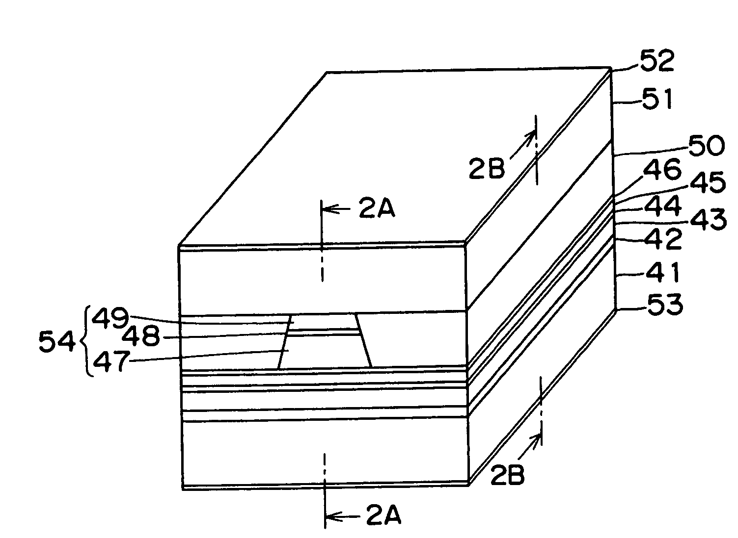
[0081]FIG. 1 is a perspective view of a semiconductor laser device according to a first embodiment of the present invention, showing a light emission end face of the device. FIG. 2A is a cross-sectional view taken along line 2A-2A of FIG. 1, showing parts including a waveguide. And, FIG. 2B is a cross-sectional view taken along line 2B-2B of FIG. 1.

[0082]In FIG. 1, reference numeral 41 denotes an n-type GaAs substrate (carrier concentration: 2×1018 cm−3), reference numeral 42 denotes an n-type GayInzP (0≦y, z≦1) buffer layer (carrier concentration: 1×1018 cm−3, y=0.515, z=0.485, film thickness: about 0.2 μm), and reference numeral 43 denotes an n-type AlxGayInzP (0≦x≦1) first cladding layer (carrier concentration: 1×1018 cm−3, x=0.360, y=0.155, z=0.485, film thickness: about 2 μm) . Reference numeral 44 denotes an active layer (MQW active layer) constructed of a multiquantum well structure of alternating AlxGayInzP barrier layers (x=0.258, y=0.257, z=0.485; each having a film thickn...

second embodiment

[0104]FIG. 5 is a perspective view of a semiconductor laser device according to a second embodiment of the present invention, showing a light emission end face of the device. FIG. 6A is a cross-sectional view taken along line 6A-6A of FIG. 5, showing parts including a waveguide. And, FIG. 6B is a cross-sectional view taken along line 6B-6B of FIG. 5.

[0105]In FIG. 5, reference numeral 61 denotes an n-type GaAs substrate (carrier concentration: 2×1018 cm−3), reference numeral 62 denotes an n-type GayInzP (0≦y, z≦1) buffer layer (carrier concentration: 1×1018 cm−3, y=0.515, z=0.485, film thickness: about 0.2 μm), and reference numeral 63 denotes an n-type AlxGayInzP (0≦x≦1) first cladding layer (carrier concentration: 1×1018 cm−3, x=0.360, y=0.155, z=0.485, film thickness: about 2 μm). Reference numeral 64 denotes an active layer (MQW active layer) constructed of a multiquantum well structure of alternating AlxGayInzP barrier layers (x=0.258, y=0.257, z=0.485; each having a film thickn...

third embodiment

[0136]FIG. 9 is a perspective view of a semiconductor laser device according to a second embodiment of the present invention, showing a light emission end face of the device. FIG. 10A is a cross-sectional view taken along line 10A-10A of FIG. 9, showing parts including a waveguide. And, FIG. 10B is a cross-sectional view taken along line 10B-10B of FIG. 9.

[0137]In FIG. 9, reference numeral 81 denotes an n-type GaAs substrate (carrier concentration: 2×1018 cm−3), reference numeral 82 denotes an n-type GayInzP (0≦y, z≦1) buffer layer (carrier concentration: 1×1018 cm−3, y=0.515, z=0.485, film thickness: about 0.2 μm), and reference numeral 83 denotes an n-type AlxGayInzP (0≦x≦1) first cladding layer (carrier concentration: 1×1018 cm−3, x=0.360, y=0.155, z=0.485, film thickness: about 2 μm). Reference numeral 84 denotes an active layer (MQW active layer) constructed of a multiquantum well structure of alternating AlxGayInzP barrier layers (x=0.258, y=0.257, z=0.485; each having a film ...


PUM


Abstract

In an AlGaInP semiconductor laser device, at least a first conductivity type first cladding layer, an active layer and a second conductivity type second cladding layer are formed on a semiconductor substrate. The second cladding layer forms a stripe-shaped ridge on a side opposite from the substrate, and a first conductivity type current block layer is disposed on both sides of the ridge. The first conductivity type current block layer has a lattice mismatch rate of −0.20% or more but not more than 0% relative to the semiconductor substrate. The lattice mismatch rate may be uniform within the current block layer. Alternatively, the lattice mismatch rate may increase continuously or stepwise with an increasing distance from a portion of the second conductivity type second cladding layer other than the ridge.

Description

[0001]This nonprovisional application claims priority under 35 U.S.C. §119(a) on Patent Application No(s). 2003-277410 filed in Japan on Jul. 22, 2003, the entire contents of which are hereby incorporated by reference.BACKGROUND OF THE INVENTION[0002]The present invention relates to a semiconductor laser device to be used for optical disks, and the like, and a method of producing the same. Particularly, the present invention relates to a semiconductor laser device having a window structure, which is superior in high power operation characteristics, and a method of producing the same.[0003]In recent years, various types of semiconductor lasers have widely been used as light sources for optical disc devices. In particular, high-power semiconductor lasers have been used as light sources for writing information to disks in a DVD (digital versatile disc) player and a CD-RAM (random access memory) drive, and there is a need for reduction of driving current and further improvement in power...

Claims


Application Information

Patent Timeline
Patent Type & Authority Patents(United States)
IPC IPC(8): H01S5/00H01S5/16H01S5/22H01S5/227H01S5/30H01S5/323
CPCH01S5/22H01S5/164H01S5/2205H01S5/168
Inventor OHKUBO, NOBUHIRO
Owner SHARP KK
Why Eureka
Try Eureka