
Phase-change material layer and phase-change memory device including the phase-change material layer

a memory device and phase-change material technology, applied in semiconductor devices, digital storage, instruments, etc., can solve the problems of reducing the data retention characteristics the loss of data stored in the volatile semiconductor memory device, and the inability of the pram device to have desired electrical characteristics, etc., to achieve the effect of reducing the driving current, increasing the set resistance, and reducing the electrod

Active Publication Date: 2010-09-07
SAMSUNG ELECTRONICS CO LTD
View PDF12 Cites 11 Cited by
  • Summary
  • Abstract
  • Description
  • Claims
  • Application Information

AI Technical Summary

Benefits of technology

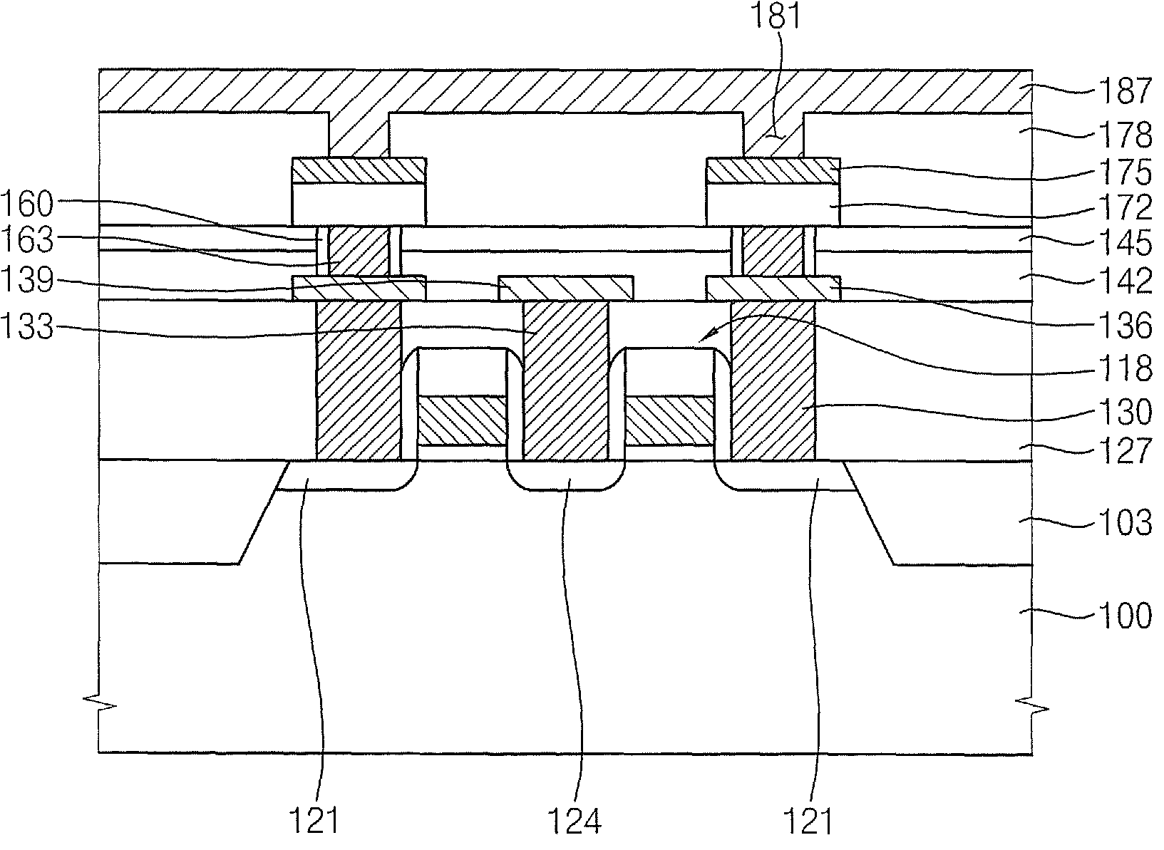
[0059]According to the present invention, a phase-change material layer or a phase-change material layer pattern may be formed using a chalcogenide compound doped with carbon and at least one of nitrogen and metal. When a phase-change memory device includes the phase-change material layer pattern, the phase-change memory device may have a considerably reduced driving current without increasing a set resistance thereof. Since the phase-change material layer pattern may provide an improved interface relative to a lower electrode and / or an upper electrode, an adhesion strength of the phase-change material layer pattern, the lower electrode and / or the upper electrode may be considerably enhanced. Additionally, a contact resistance between the phase-change material layer pattern and the electrode may be greatly increased. When the phase-change material layer pattern includes the chalcogenide compound doped with carbon and at least one of nitrogen and metal, the phase-change material layer pattern may have an increased crystallization temperature so as to ensure a high transition temperature of the phase-change material layer pattern. Further, the phase-change memory device including the phase-change material layer pattern may have improved data retention characteristics.

Problems solved by technology

The volatile semiconductor memory device loses data stored therein when power is off.
However, the non-volatile semiconductor memory device keeps stored data even if power is out.
In the conventional PRAM device, however, the phase-change material layer may not have proper properties so that the PRAM device may not have desired electrical characteristics.
For example, the phase-change material layer may be rapidly deteriorated, to thereby considerably reduce data retention characteristics of the PRAM device.
Further, the phase-change memory device of GST compound doped with nitrogen may not ensure good adhesion strength relative to the first electrode and the second electrode.

Method used


Image

  • Phase-change material layer and phase-change memory device including the phase-change material layer
  • Phase-change material layer and phase-change memory device including the phase-change material layer
  • Phase-change material layer and phase-change memory device including the phase-change material layer

Examples


Embodiment Construction

[0072]The present invention is described more fully hereinafter with reference to the accompanying drawings, in which example embodiments of the present invention are shown. The present invention may, however, be embodied in many different forms and should not be construed as limited to the example embodiments set forth herein. Rather, these example embodiments are provided so that this disclosure will be thorough and complete, and will fully convey the scope of the present invention to those skilled in the art. In the drawings, the sizes and relative sizes of layers and regions may be exaggerated for clarity.

[0073]It will be understood that when an element or layer is referred to as being “on,”“connected to” or “coupled to” another element or layer, it can be directly on, connected or coupled to the other element or layer or intervening elements or layers may be present. In contrast, when an element is referred to as being “directly on,”“directly connected to” or “directly coupled ...


PUM

PropertyMeasurementUnit
widthaaaaaaaaaa
set resistancesaaaaaaaaaa
widthaaaaaaaaaa

Abstract

A phase-change memory device includes a substrate having a contact region, an insulating interlayer on the substrate, a lower electrode electrically connected to the contact region, a phase-change material layer pattern formed on the lower electrode, and an upper electrode formed on the phase-change material layer pattern. The phase-change material layer pattern includes a chalcogenide compound doped with carbon and at least one of nitrogen and metal. The phase-change memory device may have a considerably reduced driving current without increasing a set resistance thereof. Further, the phase-change material layer pattern may have an increased crystallization temperature so as to ensure improved data retention characteristics of the phase-change memory device.

Description

CROSS-REFERENCE TO RELATED APPLICATION[0001]This application claims priority under 35 USC §119 to Korean Patent Application No. 2006-94208 filed on Sep. 27, 2006, the contents of which are incorporated herein by reference in their entirety.FIELD OF THE INVENTION[0002]Example embodiments of the present invention relate to a phase-change material layer and a phase-change memory device. More particularly, example embodiments of the present invention relate to a phase-change material layer including a chalcogenide compound doped with carbon and at least one of nitrogen and metal, and a phase-change memory device having the phase-change material layer.BACKGROUND OF THE INVENTION[0003]Semiconductor memory devices are generally divided into volatile semiconductor memory devices such as dynamic random access memory (DRAM) devices or static random access memory (SRAM) devices, and non-volatile semiconductor memory devices such as flash memory devices or electrically erasable programmable rea...

Claims


Application Information

Patent Timeline
Patent Type & Authority Patents(United States)
IPC IPC(8): G11C11/00
CPCH01L27/2409H01L27/2436H01L45/06H01L45/1233H01L45/143H01L45/144H01L45/1616H01L45/1625H01L45/1675H01L45/1683H10B63/20H10B63/30H10N70/231H10N70/8825H10N70/826H10N70/8828H10N70/026H10N70/023H10N70/066H10N70/063
Inventor KUH, BONG-JINHA, YONG-HOKO, HAN-BONGPARK, DOO-HWANSHIN, HEE-JULIM, SANG-WOOK
Owner SAMSUNG ELECTRONICS CO LTD
Learn More