Micro-machined imaging interferometer

a micro-machined optical measuring and interferometer technology, applied in the direction of optical radiation measurement, interferometric spectrometry, instruments, etc., can solve the problems of delicate polishing step and problematic production of such a devi

Active Publication Date: 2012-12-27
COMMISSARIAT A LENERGIE ATOMIQUE ET AUX ENERGIES ALTERNATIVES +1
View PDF8 Cites 0 Cited by
  • Summary
  • Abstract
  • Description
  • Claims
  • Application Information

AI Technical Summary

Benefits of technology

[0016]Said first face of the second support can have undergone an anti-reflection treatment. Such a treatment is provided so as to increase the transmission coefficient, on one hand, and on the other hand, to prevent multiple reflections of the light in the second support. Such a treatment can be done by deposition of an anti-reflection layer, for example ZnS-based in the case of infrared applications.
[0035]The preceding devices offer the possibility of going from an interferometric device to a device able to measure the interferograms produced in said cavity and / or study the spectral properties of the waves forming the interference figures, without modifying the structure or geometry of the devices.

Problems solved by technology

However, the production of such a device is problematic.
This polishing step is delicate, inasmuch as it involves making a planar surface at the end of the manufacturing process, without destroying the detection zone of the imager.
However, if this polishing step is not done correctly, the entire manufacturing process must be reiterated, including the production of the imager.
The problem arises of finding a new way of making a micro-machined optical measuring device co-integrating an interferometer function and an imaging function, and that does not require a transfer lens between the element performing the function of interferometer and the imager.

Method used


Image

  • Micro-machined imaging interferometer
  • Micro-machined imaging interferometer
  • Micro-machined imaging interferometer

Examples


Embodiment Construction

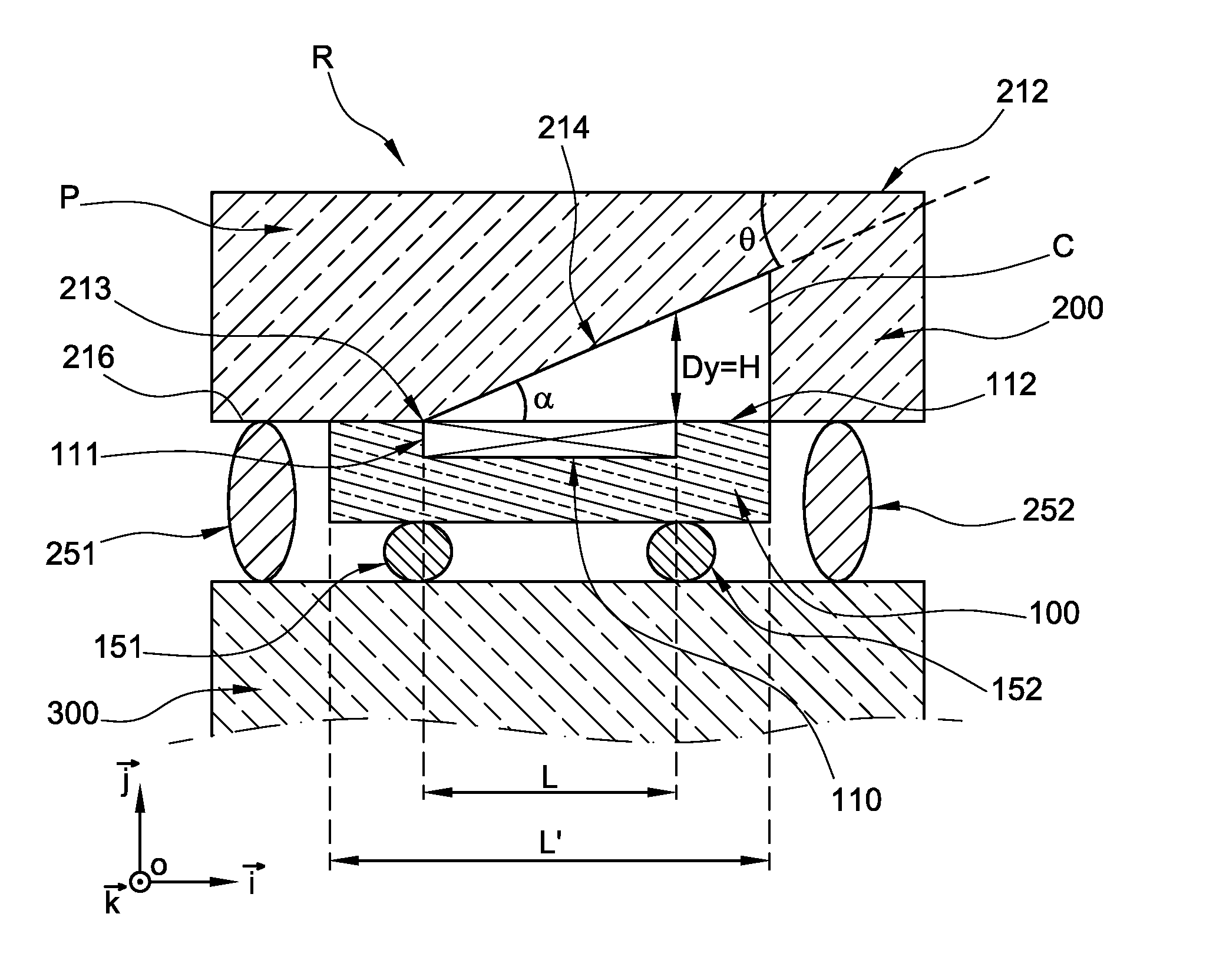
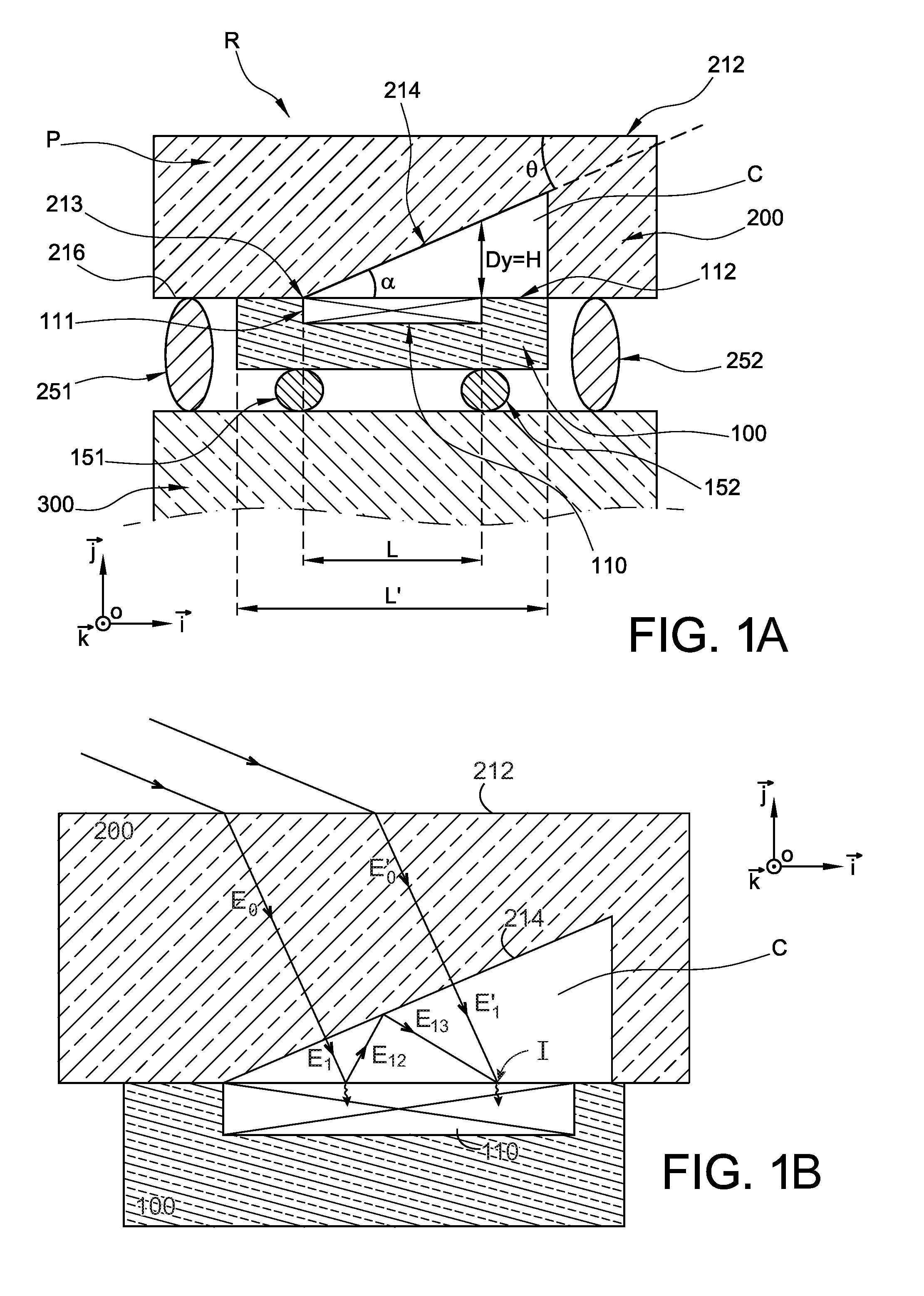
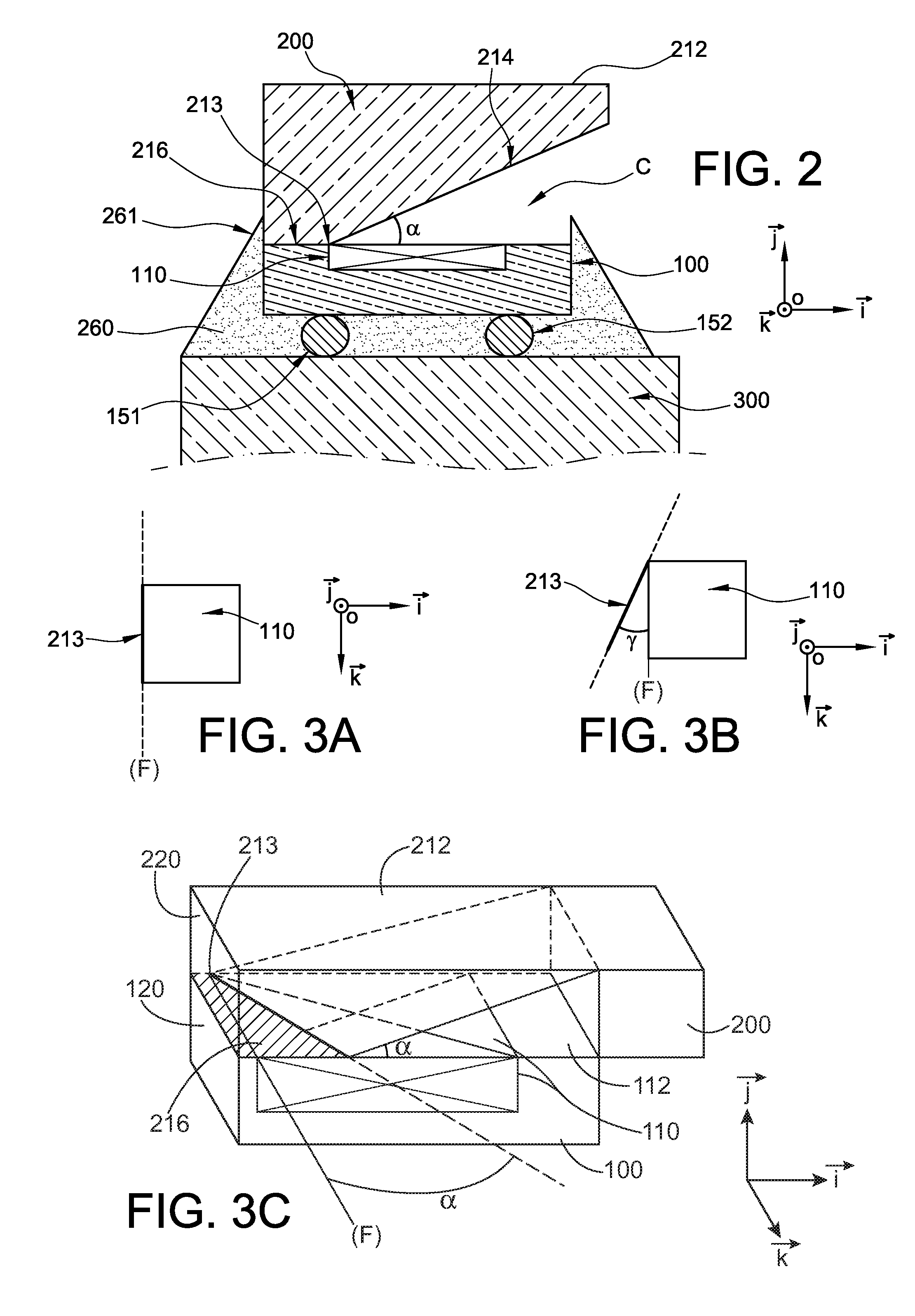
[0043]An example of a micro-machined optical measuring device according to the invention will now be provided in connection with FIG. 1.

[0044]This device comprises an electromagnetic radiation detector imager, formed on a first support 100, which can be a semiconducting substrate, for example with a base of CdHgTe in the case of an infrared detector.

[0045]The imager is provided with a plurality of photosensitive detector elements 110 formed on the substrate and positioned on a given face 112 thereof. The surface of the photodetectors is semi-reflective. The imager can, for example, be an imager intended to detect radiation between the ultraviolet and the far infrared. The spectral band detected by the photosensitive detector elements is between a maximum wavelength that can be set by the characteristics of the photosensitive detectors, and a minimum wavelength defined by the optical transmission characteristics of the elements positioned on the optical path of the light, upstream of...


PUM


Abstract

A micro-machined optical measuring device including: a set of photosensitive detector elements situated on a given face of a first support; a second support, assembled to the first support, forming a prism and including a first face through which a visible radiation is intended to penetrate and a second face, forming a non-zero angle θ with the first face and a non-zero angle α with the given face of the first support, the second face being semi-reflective, the first support and the second support being positioned such that an interferometric cavity is made between the second face and the given face, the distance between the given face of the first support and the second face of the second support varying regularly.

Description

TECHNICAL FIELD[0001]The present invention relates to the field of micro-machined optical measuring devices and in particular that of spectrometer devices, provided with co-integrated static interferometer and imaging functions.BACKGROUND OF THE INVENTION[0002]It is known to make micro-machined spectrometer devices.[0003]Document U.S. Pat. No. 7,330,266 B2 for example discloses a static Fourier transform spectrometer provided with an interferometer function done using a strip having a first planar face situated on the detection zone of an imager, and a second planar face, which is inclined relative to the first planar face, and performs a semi-reflective diopter function. The strip is formed from the substrate on which the imaging was done.[0004]An interferogram, mapping of the interferences that occur, is obtained in a single acquisition by the imager, without a transfer lens being necessary between the interferometric block and the imager. This spectrometer is pre-adjusted.[0005]H...

Claims


Application Information

Patent Timeline
Patent Type & Authority Applications(United States)
IPC IPC(8): G01J3/45
CPCG01J3/02G01J3/021G01J3/0256G01J3/4531G01J3/26G01J3/2823G01J3/0259H01L2224/16225
Inventor FENDLER, MANUELLAFARGUES, GILLESGUERINEAU, NICOLASROMMELUERE, SYLVAINDE LA BARRIERE, FLORENCE
Owner COMMISSARIAT A LENERGIE ATOMIQUE ET AUX ENERGIES ALTERNATIVES
Why Eureka
Try Eureka