

Pressure detecting device and method for manufacturing the same, display device and method for manufacturing the same, and TFT substrate with pressure detecting device
- Summary
- Abstract
- Description
- Claims
- Application Information
AI Technical Summary
Benefits of technology
Problems solved by technology
Method used
Image

Examples
first embodiment
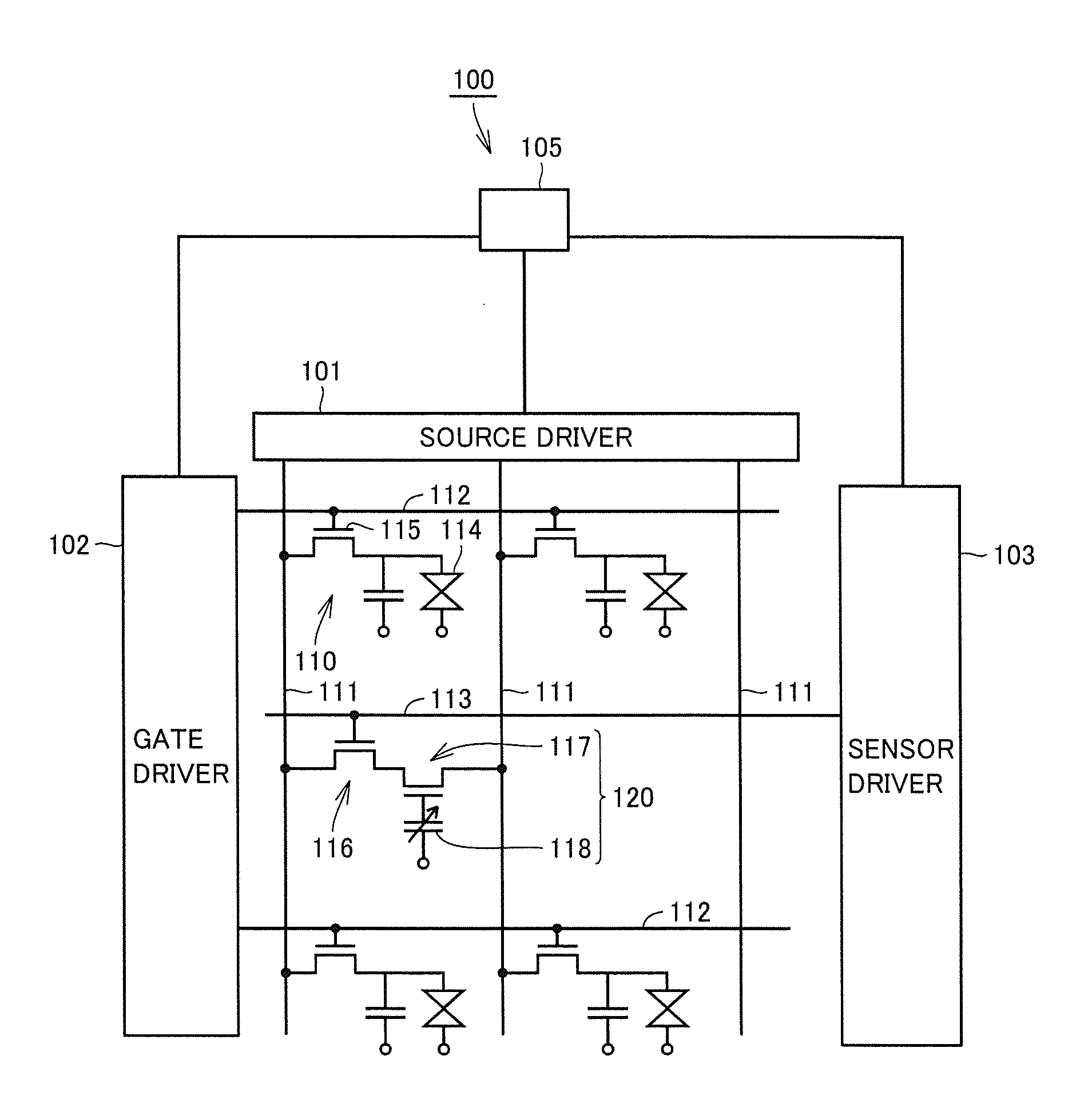
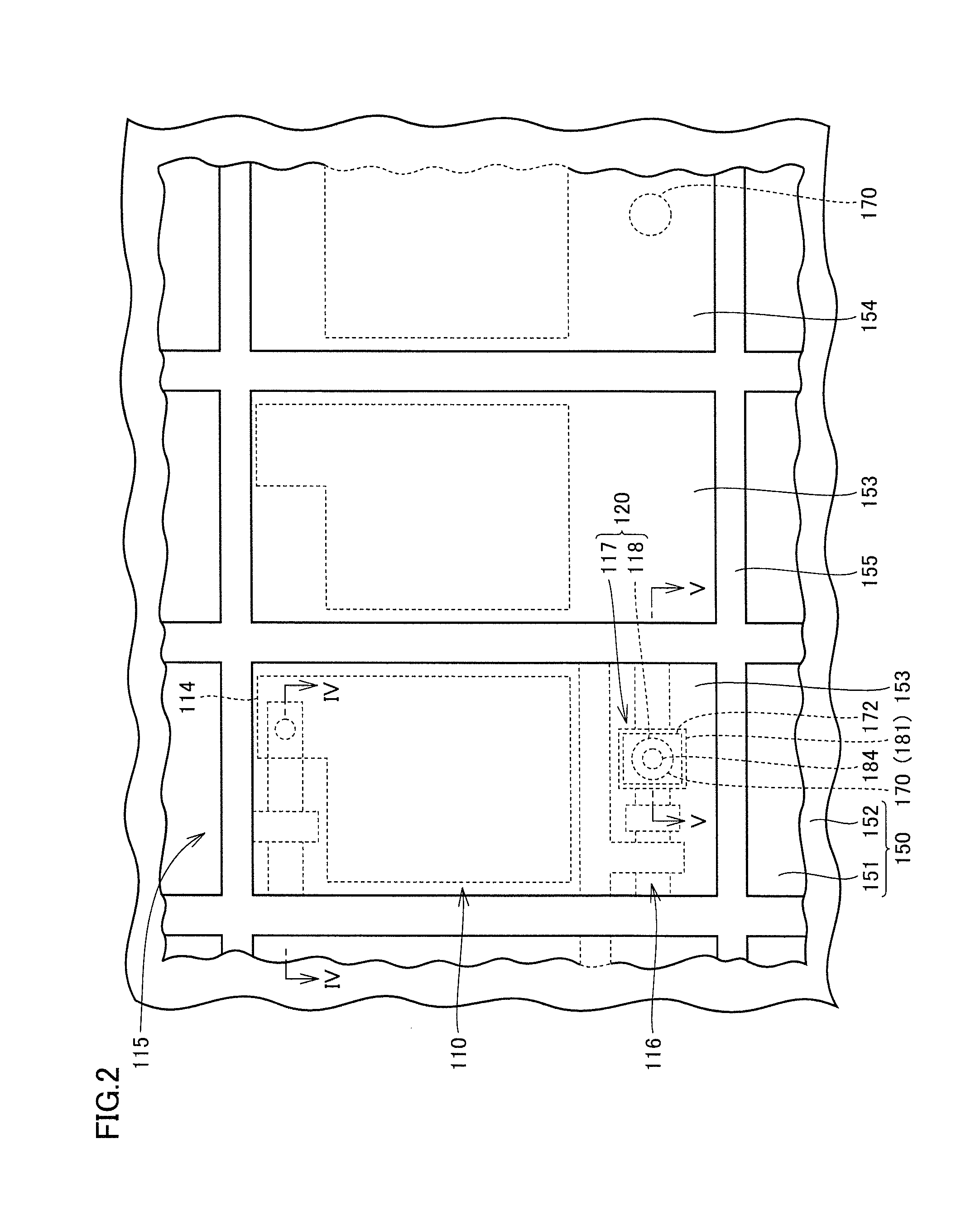
[0102]FIG. 1 is a circuit diagram schematically showing a circuit diagram of a liquid crystal display device 100 according to a first embodiment as a reference technique. As shown in this FIG. 1, liquid crystal display device 100 includes a control unit 105 and a plurality of pixels 110 arranged in an array. Pixel 110 includes a plurality of TFT (Thin Film Transistor) elements 115 and a pixel electrode 114 connected to this TFT element 115.
[0103]Liquid crystal display device 100 includes a plurality of gate lines 112 and gate lines for sensing 113 extending in a first direction and spaced apart from one another in a second direction, and a plurality of source lines 111 extending in the second direction and spaced apart from one another in the first direction.
[0104]Each gate line 112 is connected to a gate driver 102, and each source line 111 is connected to a source driver 101. Gate line for sensing 113 is arranged between adjacent gate lines 112, and the plurality of gate lines for...
second embodiment
[0210]Pressure sensor 118 and liquid crystal display device 100 according to a second embodiment of the present invention will be described with reference to FIGS. 22 to 26. The same reference characters are given to the components shown in FIGS. 22 to 26 that are the same as or corresponding to those shown in FIGS. 1 to 21 above, and description thereof will not be repeated.
[0211]FIG. 22 is a cross-sectional view of liquid crystal display device 100 according to the second embodiment and is a cross-sectional view showing TFT element 115. FIG. 23 is a cross-sectional view of liquid crystal display device 100 according to the second embodiment and is a cross-sectional view in output element 117.
[0212]As shown in these FIGS. 22 and 23, liquid crystal display device 100 includes TFT element 115 and output element 117, and interlayer dielectric 135 is formed to cover TFT element 115 and output element 117.
[0213]Upper ends of drain electrode 137 and source electrode 138 of TFT element 11...
third embodiment
[0236]Pressure sensor 118, liquid crystal display device 100 and a method for manufacturing liquid crystal display device 100 according to a third embodiment of the present invention will be described with reference to FIGS. 27 to 37. The same reference characters are given to the components shown in FIGS. 27 to 37 that are the same as or corresponding to those shown in FIGS. 1 to 26 above, and description thereof will not be repeated.
[0237]FIG. 27 is a cross-sectional view of liquid crystal display device 100 according to the third embodiment and is a cross-sectional view showing TFT element 115. FIG. 28 is a cross-sectional view of liquid crystal display device 100 according to the third embodiment and is a cross-sectional view showing pressure sensor 118.
[0238]As shown in this FIG. 27, liquid crystal display device 100 includes an underlying layer 141 formed on the main surface of glass substrate 140, underlying layer 131 formed on an upper surface of this underlying layer 141, a...
PUM
 Abstract
Description
Claims
Application Information