Method for forming copper distributing wires

a technology of distributing wires and copper, applied in the direction of resistive material coating, chemical vapor deposition coating, solid-state devices, etc., can solve the problems of difficult formation of copper distributing wires from such a plating solution, difficult to penetrate even deep depth or interior, and long size of contact holes or the like, etc., to achieve excellent step-covering ability and efficiently form a copper-containing film

Active Publication Date: 2011-10-11
ULVAC INC
View PDF15 Cites 1 Cited by
  • Summary
  • Abstract
  • Description
  • Claims
  • Application Information

AI Technical Summary

Benefits of technology

[0032]According to the present invention, a primary coat possessing an excellent step-covering ability is formed in advance when a copper-containing film is deposited by the CVD technique, as has been described above. This would permit the achievement of such an effect that holes and / or grooves (including the side walls of these holes and / or grooves), such as those each having an opening (φ) of 0.05 μm) each having a high aspect ratio (for instance, 17), are completely filled with a uniform copper-containing film without accompanying the formation of any void.
[0033]As has been discussed above, the present invention makes use, as a primary coat, of a barrier layer which can prevent any mutual diffusion of the wire material and the insulating material and / or an adherent later which can prevent any peeling of films at the boundary between the layers of the wire material and the insulating material, whereby the method of the present invention shows an effect such that it becomes possible to efficiently form a copper-containing film useful as a material for forming desired copper distributing wires. In addition, the method of the present invention also shows an effect such that the easy formation of initial nuclei at a high nuclear density required for forming a desired copper-containing film within a very short period of time and the formation of a continuous film, as well as the use of a barrier layer and / or an adherent layer which can ensure the desired excellent adhesion between the copper-containing film thus formed and the barrier and / or adherent layers as a primary coat would likewise permit the efficient formation of a copper-containing film useful as a material for forming desired copper distributing wires.

Problems solved by technology

However, the size of contact holes or the like has become longer and narrower as the reduction of the scale of the distributing wires of, for instance, LSI elements, and an additional problem arises, such that it would be difficult for a plating solution to penetrate into even the deep depth or interior of, for instance, such long and narrow contact holes having such a high aspect ratio.
Accordingly, this makes the formation of copper distributing wires from such a plating solution, quite difficult.
In the copper distributing wire-forming process, which makes use of the CVD technique, however, the formation of the copper film is greatly affected by the surface characteristic properties of the material used for forming a primary coat and more specifically, the process suffers from various problems in that (1) it is difficult to form initial nuclei and it takes a long period of time to form such initial nuclei; and (2) the film is apt to undergo the so-called island-like growth.
Accordingly, it would be quite difficult to form a continuous film by the use of the foregoing process.
Thus, any CVD technique cannot be used for filling holes or grooves each having a diameter of not more than 0.1 μm, whose filling by the plating technique becomes difficult and this would result in a serious problem in the future.
The process likewise suffers from a problem in that it is difficult to ensure any excellent adhesion between the copper-containing film formed through the CVD technique and a barrier layer or the like.
In this case, bis(cyclopenta-dienyl) vanadium(III) is, for instance, used as a raw material for forming a barrier layer, but any satisfactory barrier layer has not always been prepared.
The conventionally used Cu(hfac)(tmvs) described above suffers from additional problems such that any desired copper-containing film cannot be prepared in good reproducibility (any stable filling of, for instance, holes cannot be ensured when the size of the opening of the hole: φ is not more than 0.2 μm and when the aspect ratio is not less than 4), which would possibly be resulted from the characteristic properties of the primary coat, and that voids are generated due to the annealing treatment after the step of filling the holes or the like.
When forming copper distributing wires, the foregoing problems would arise and accordingly, the conventional techniques would never produce any LSI element provided with highly reliable distributing wires.
When using the copper complex, however, there are many problems remaining unsolved.

Method used


Image

  • Method for forming copper distributing wires
  • Method for forming copper distributing wires
  • Method for forming copper distributing wires

Examples


example 1

[0060]In this Example, a barrier layer consisting of vanadium nitride was formed while variously changing the barrier layer-forming conditions and then a copper-containing film was deposited on the barrier layer to thus variously investigate the initial nucleation conditions.

Step 1:

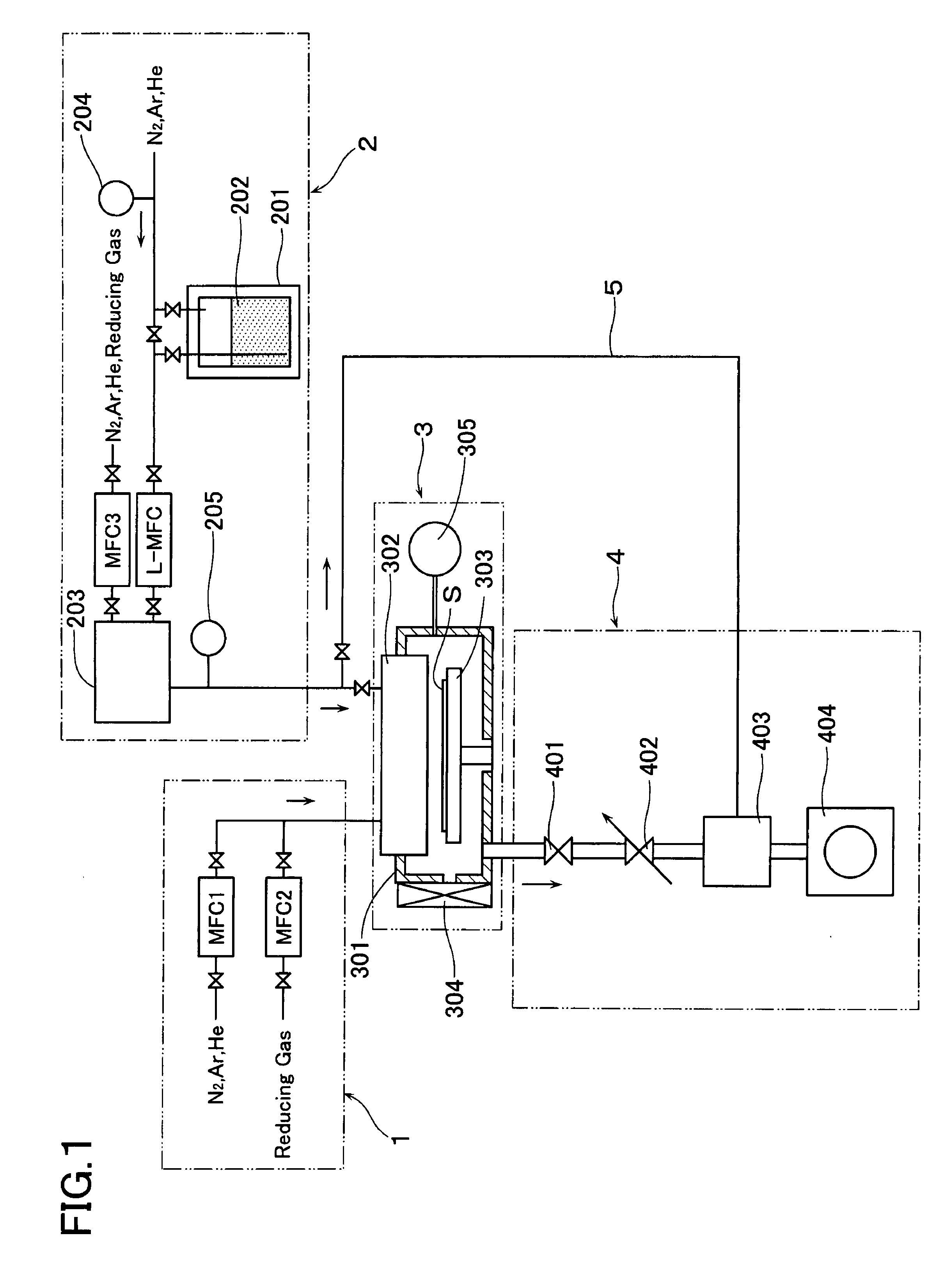
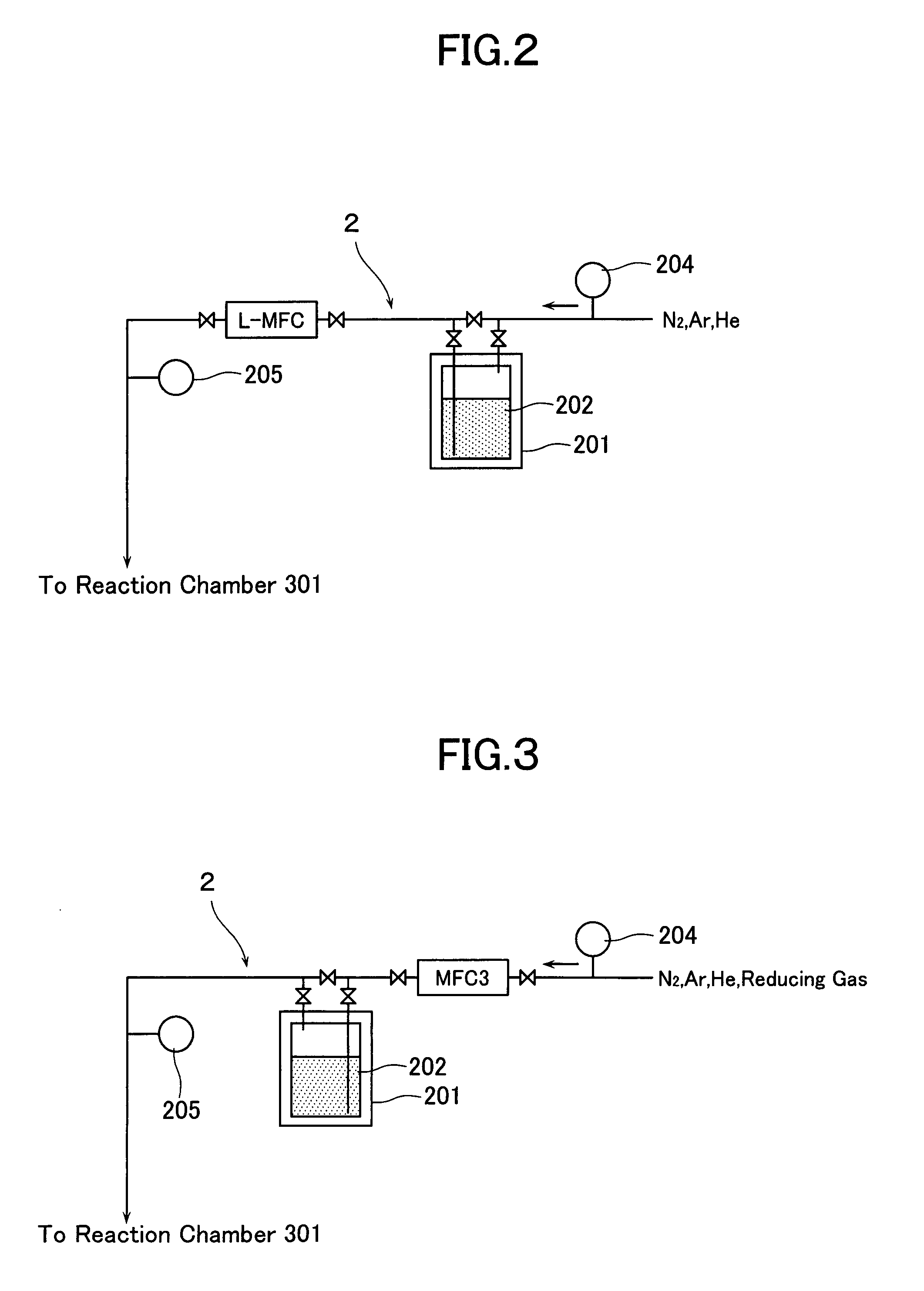
[0061]A vanadium-containing film was formed on the surface of a substrate S using the CVD apparatus as shown in FIG. 1. In this respect, the substrate S used herein was a wafer (SiO2 / Si) having a diameter of 8 inches, on which a silicon oxide film had been formed.

[0062]The gate valve 304 of the reaction device 3 was opened and then the substrate S was conveyed into the reaction chamber 301 using a robot positioned in the chamber in the proximity of the reaction chamber. The conveyance of the substrate is desirably carried out in a vacuum for the prevention of any adhesion, onto the surface of the substrate, of gases present in the air, for instance, carbon atom-containing gases (such as CO or CO2), oxygen...

example 2

[0158]A vanadium-containing film was formed on the surface of a substrate S using the CVD apparatus as shown in FIG. 1. In this respect, the substrate S used herein was a wafer (SiO2 / Si) having a diameter of 8 inches, on which a silicon oxide film had been formed and then holes and / or grooves having a variety of sizes were formed.

[0159]The gate valve 304 of the reaction device 3 was opened and then the substrate S was conveyed into the reaction chamber 301 using a robot positioned in the chamber in the proximity to the reaction chamber. The conveyance of the substrate is desirably carried out in a vacuum for the prevention of any adhesion, onto the surface of the substrate, of gases present in the air such as carbon atom-containing gases (such as CO or CO2), oxygen-containing gases (such as O2), and water (H2O) or for the prevention of any diffusion or penetration of these gases into the interior of the substrate. Accordingly, the substrate was conveyed into the reaction chamber und...

example 3

[0187]The process for filling holes and / or grooves with a copper-containing film will be described in this Example, while using the substrate provided thereon with a barrier layer and prepared in Example 2.

[0188]The following film-forming processes were carried out using the CVD apparatus as shown in FIG. 1. The substrate provided thereon with the vanadium-containing film prepared in Example 2 was conveyed to a copper-containing film-forming reaction chamber through a transportation chamber (maintained at a vacuum) arranged in the proximity of the reaction chamber 301, while paying much attention not to expose the substrate to the air for the prevention of any oxidation of the surface thereof, followed by placing the substrate on the substrate-placing table 303 maintained at a predetermined temperature. Separately, an SiO2 / Si substrate free of any vanadium-containing film was likewise placed on the substrate-placing table 303 of the copper-containing film-forming reaction chamber 30...


PUM

PropertyMeasurementUnit
temperatureaaaaaaaaaa
widthaaaaaaaaaa
aspect ratioaaaaaaaaaa

Abstract

A method of forming a primary coat, which consists of a V- or Ti-containing film, formed on the surface of a subject on which holes or the like have been formed, according to the CVD technique, while using, for instance, a tetravalent amide-type vanadium-containing organometal compound as a raw gas and using, for instance, tertiary butyl hydrazine as a reducing gas, and a copper-containing film is then formed on the primary coat, according to the CVD technique, to thus fill the holes or the like with the copper-containing film and to thus form copper distributing wire, which is excellent in the hole-filling properties and excellent in the adhesion to a primary coat, this process can be applied to the field of copper distributing wires used in the semiconductor industries.

Description

CROSS-REFERENCE TO RELATED APPLICATION[0001]This application is a National Stage entry of International Application Number PCT / JP2005 / 016712, filed Sep. 12, 2005. The disclosure of the prior application is hereby incorporated herein in its entirety by reference.TECHNICAL FIELD[0002]The present invention relates to a method for forming copper distributing wires or copper interconnections and, in particular, to a method for forming copper distributing wires, which comprises the step of forming a copper-containing film, by the CVD technique, on a primary coat or under coat consisting of a vanadium- or titanium-containing film formed according to the CVD technique.BACKGROUND ART[0003]With respect to the distributing wires required when fabricating a semiconductor element (such as an LSI or IC element or the like), it is common that a barrier and / or adherent layer as a primary coat in or on contact holes and grooves which permit the connection between lower and upper distributing wires. ...

Claims


Application Information

Patent Timeline
Patent Type & Authority Patents(United States)
IPC IPC(8): B05D5/12
CPCC07C49/92C23C16/0272C23C16/045C23C16/18C23C16/34H01L21/28556H01L21/76843H01L21/76877H01L23/5226H01L23/53238H01L2924/0002H01L2924/00H01L21/3205
Inventor WATANABE, MIKIOZAMA, HIDEAKI
Owner ULVAC INC
Why Eureka
Try Eureka