

Touch panel and method of detecting coordinate position
a technology of coordinate position and touch panel, which is applied in the direction of electronic switching, pulse technique, instruments, etc., can solve the problems of increased thickness and higher cost, and achieve the effect of increasing thickness and higher cos
- Summary
- Abstract
- Description
- Claims
- Application Information
AI Technical Summary
Benefits of technology
Problems solved by technology
Method used
Image

Examples
first embodiment
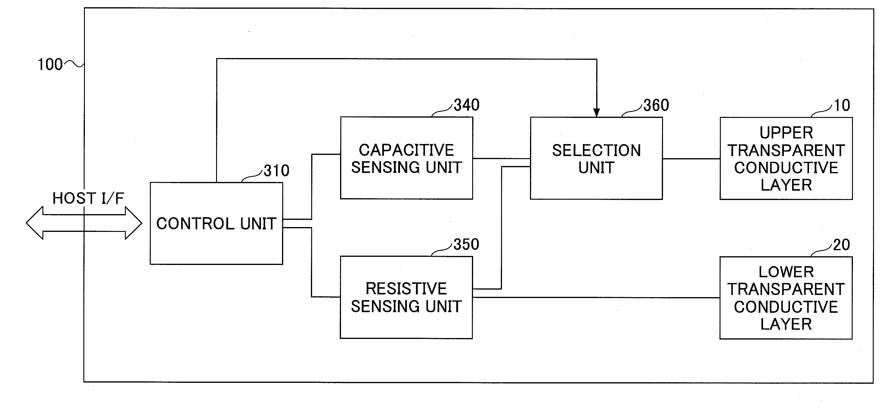
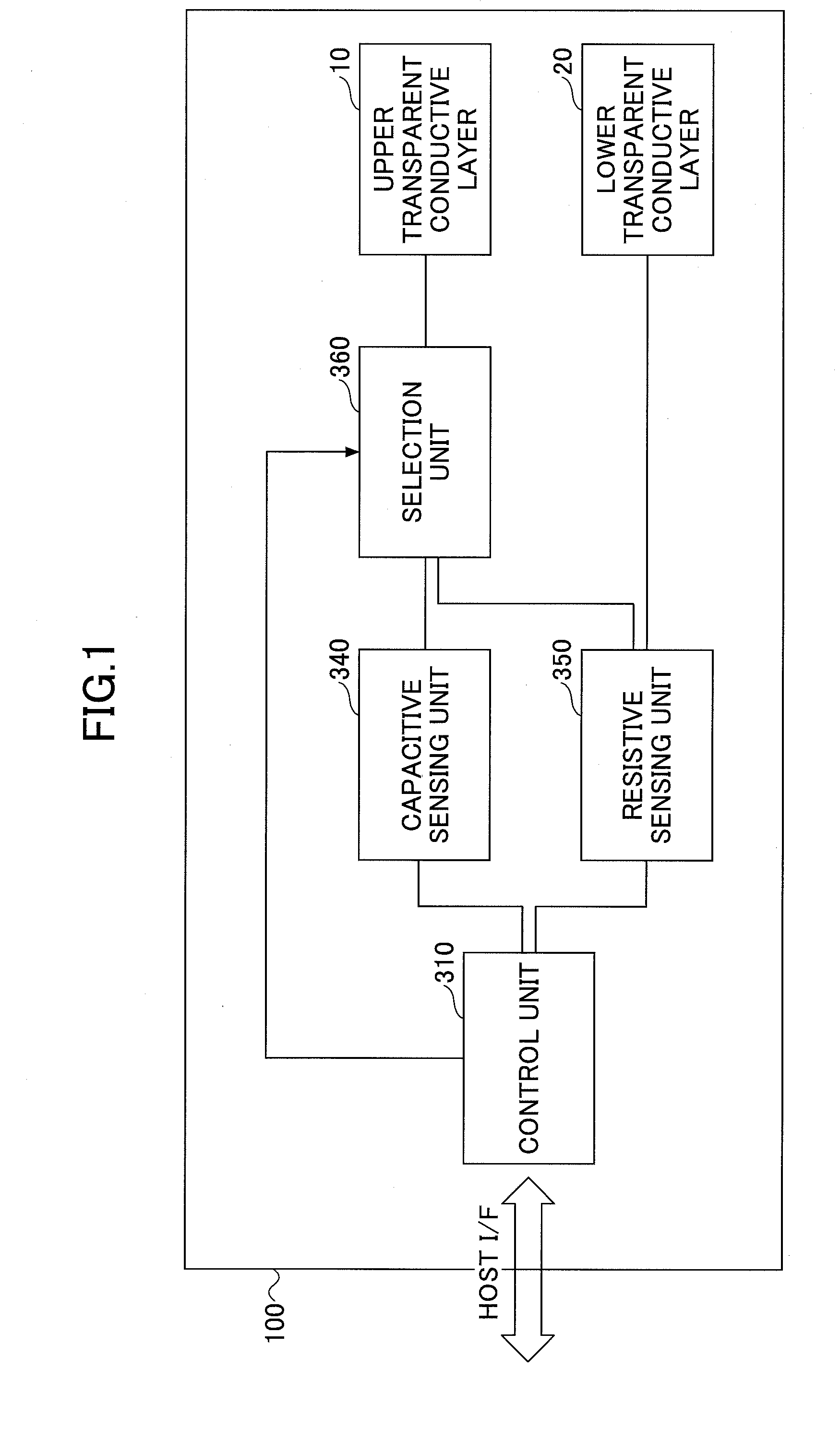
[0047]A touch panel of a first embodiment will be explained.
[0048]FIG. 2 is an explanatory view showing an example of a structure of a touch panel 100 of the embodiment.
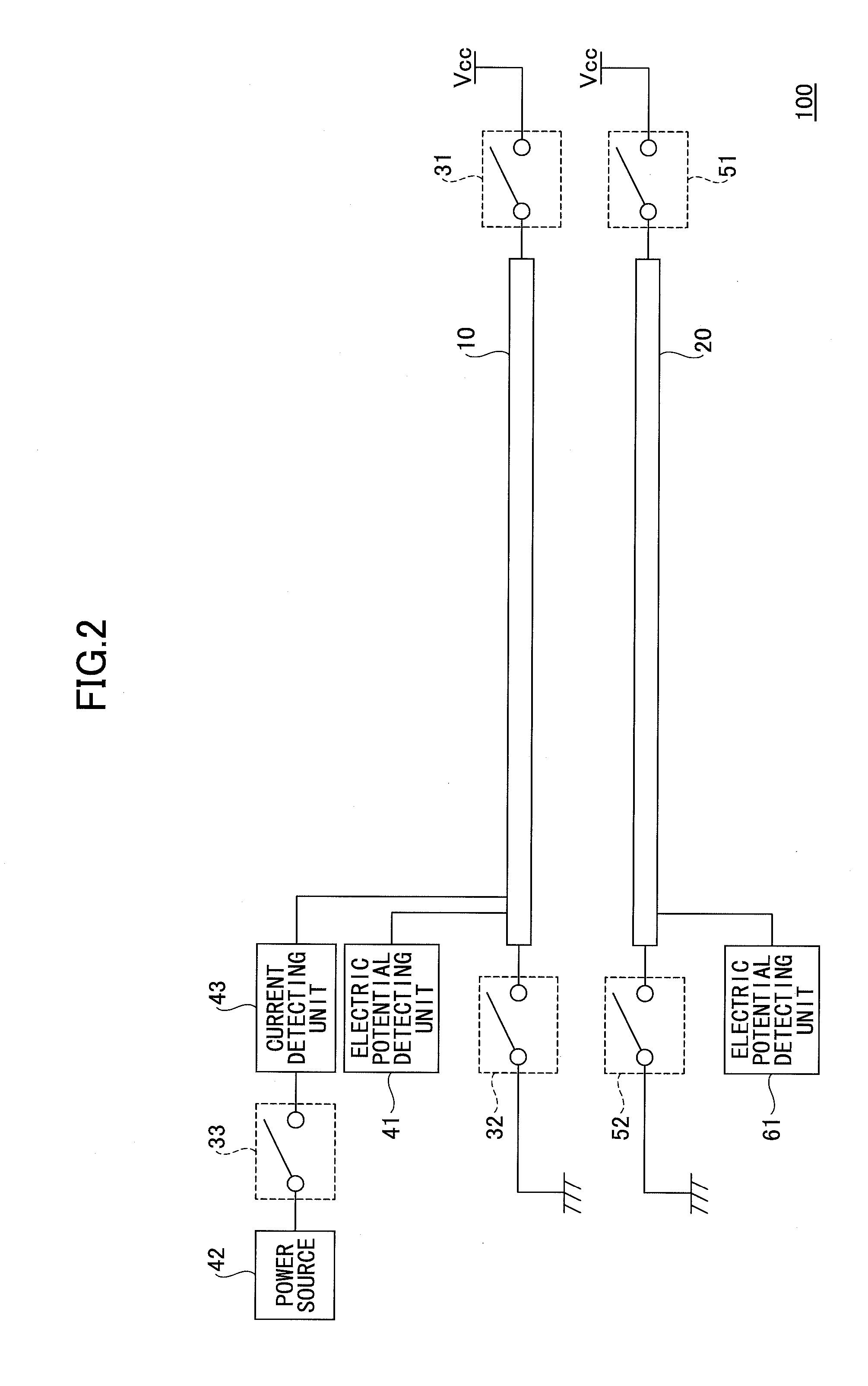
[0049]The touch panel 100 of the embodiment is a four-wire type. The touch panel 100 includes an upper transparent conductive layer 10 formed on an upper conductive substrate (not shown in FIG. 2), and a lower transparent conductive layer 20 formed on a lower conductive substrate (not shown in FIG. 2). The upper conductive substrate is composed of a transparent film or the like. The lower conductive substrate is composed of a glass or the like. The upper transparent conductive layer 10 and the lower transparent conductive layer 20 are positioned to face each other with a predetermined interval.
[0050]The touch panel 100 further includes switches 31 and 32 respectively connected to opposing edges in an X-axis direction of the upper transparent conductive layer 10. The switch 31 is connected to a power source (not shown...
second embodiment
[0106]A touch panel of a second embodiment will be explained.
[0107]FIG. 12 is an explanatory view showing an example of a structure of a touch panel 100 of the embodiment.
[0108]The touch panel 100 of the embodiment is a five-wire type.
[0109]The touch panel 100 includes an upper transparent conductive layer 110 formed on an upper conductive substrate (not shown in FIG. 12), and a lower transparent conductive layer 120 formed on a lower conductive substrate (not shown in FIG. 12). The upper transparent conductive layer 110 and the lower transparent conductive layer 120 are positioned to face each other with a predetermined interval.
[0110]The touch panel 100 further includes switches 151 and 152 respectively connected to a power source (not shown in the drawings) to be provided with a power source potential (Vcc) and a ground potential.
[0111]The switch 151 includes a first terminal 151a and a second terminal 151b respectively connected to the lower transparent conductive layer 120. The...
PUM
 Abstract
Description
Claims
Application Information