Non-polar light emitting diode having photonic crystal structure and method of fabricating the same

a technology of light-emitting diodes and photonic crystals, which is applied in the manufacture of semiconductor/solid-state devices, semiconductor devices, electrical devices, etc., can solve the problems of limited improvement in light-emitting efficiency, reduced emitting recombination rate, and difficulty in increasing the thickness of well-layered layers, etc., to achieve the effect of improving light-emitting efficiency

Inactive Publication Date: 2013-01-31
SEOUL VIOSYS CO LTD
View PDF7 Cites 30 Cited by
  • Summary
  • Abstract
  • Description
  • Claims
  • Application Information

AI Technical Summary

Benefits of technology

[0010]Exemplary embodiments of the present invention provide a non-polar light emitting diode (LED) having an improved light emitting efficiency and a method of fabricating the same.
[0011]Exemplary embodiments of the present invention also provide a non-polar LED having a new structure and a method of fabricating the same, thereby capable of improving the polarization ratio of the light emitted from the non-polar LED.
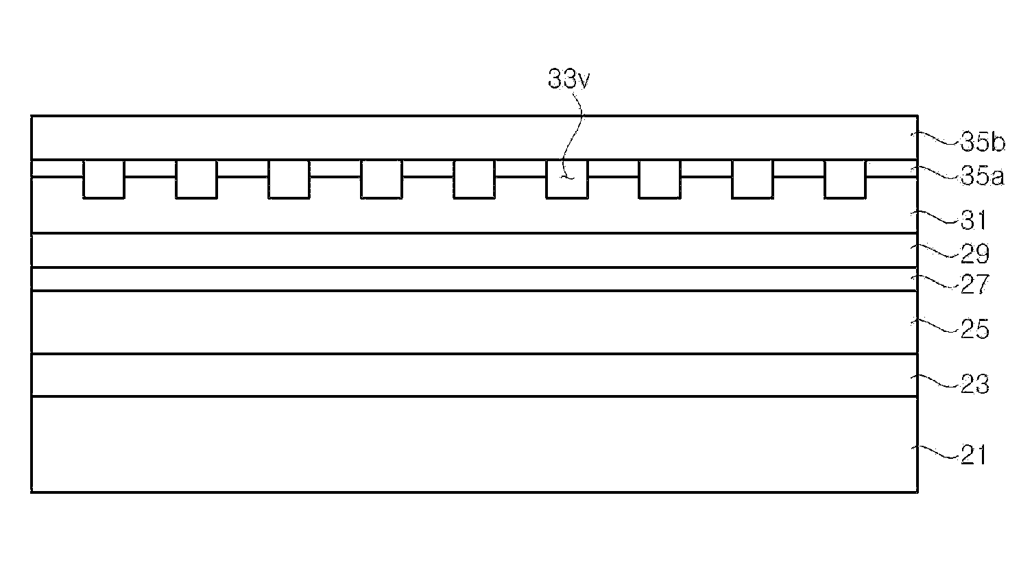
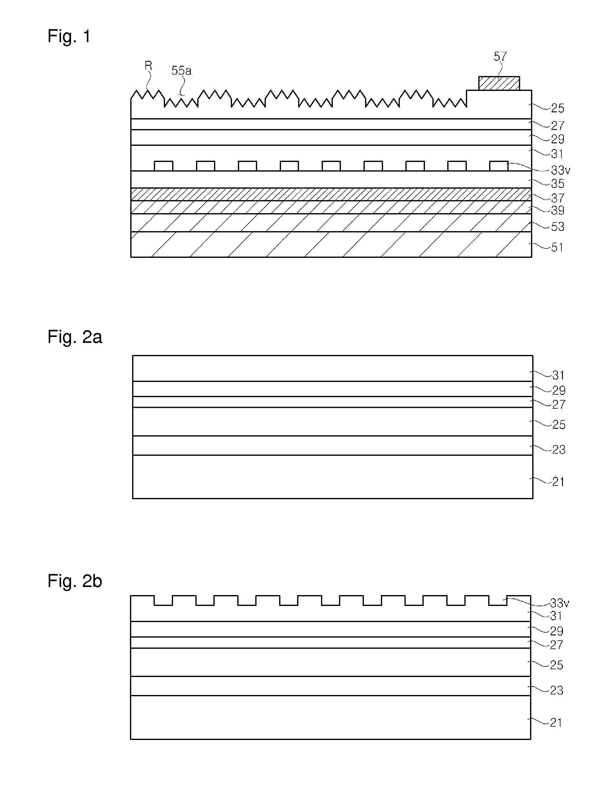
[0013]An exemplary embodiment of the present invention discloses a non-polar LED, the non-polar LED including: a support substrate; a lower semiconductor layer disposed on the support substrate; an upper semiconductor layer disposed over the lower semiconductor layer; an active region disposed between the lower and upper semiconductor layers; and a photonic crystal structure embedded in the lower semiconductor layer. The photonic crystal structure may improve the light emitting efficiency by preventing the loss of light in the semiconductor layers, and improve the polarization ratio of the non-polar LED.
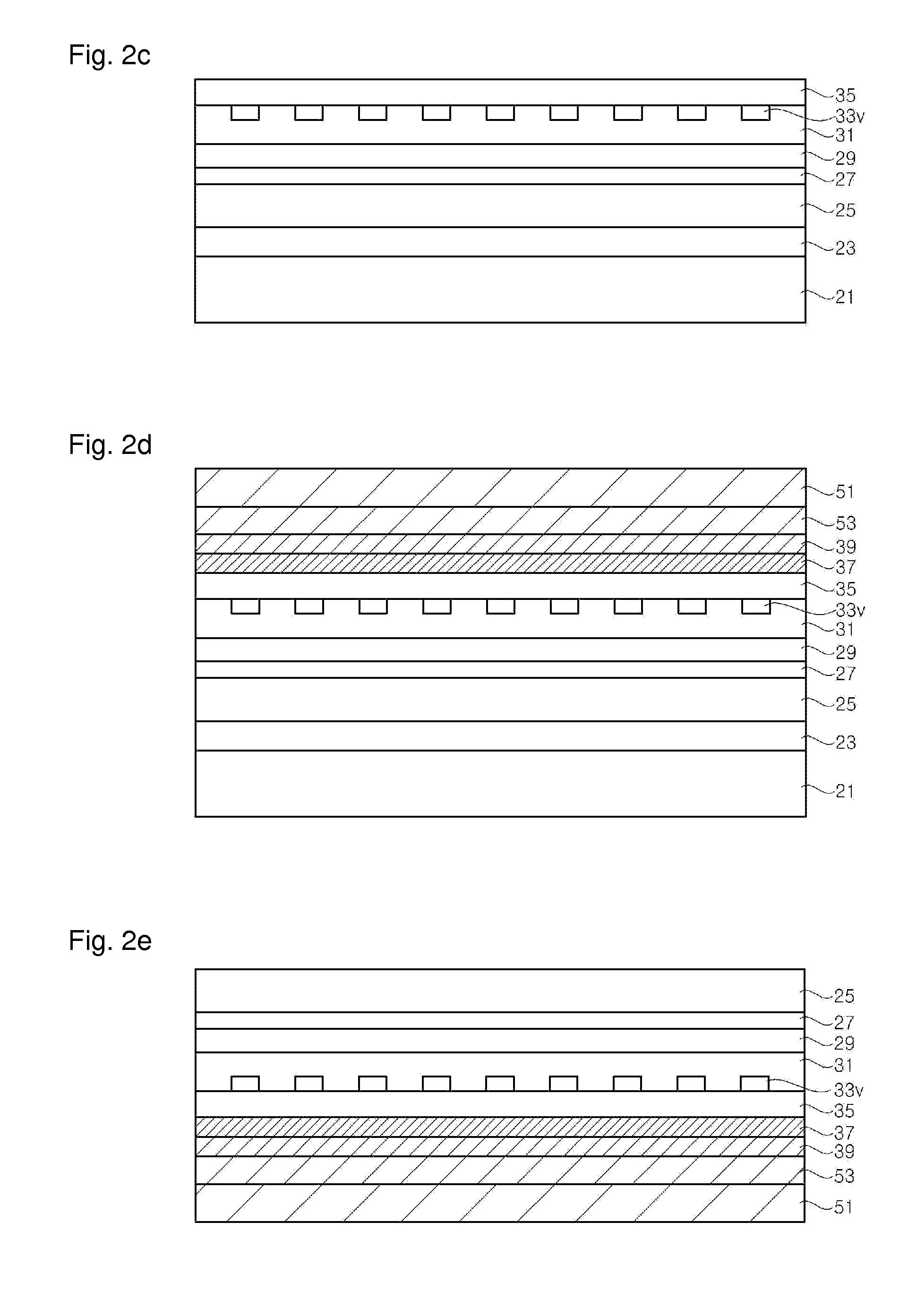
[0014]An exemplary embodiment of the present invention also discloses a method of fabricating a non-polar LED, the method including: forming a first conductive semiconductor layer, a non-polar active region and a second conductive semiconductor layer on a growth substrate; forming a pattern of voids by partially patterning the second conductive semiconductor layer; forming a second conductive contact layer for covering the pattern of the voids; forming an ohmic contact layer on the second conductive contact layer; forming a support substrate on the ohmic contact layer; and removing the growth substrate and exposing the first conductive semiconductor layer. A photonic crystal structure is provided by the pattern of the voids, and thus it is possible to fabricate the non-polar LED having the photonic crystal structure embedded in the lower semiconductor layer between the support substrate and the non-polar active region.

Problems solved by technology

A strong polarization field is generated in an active region having a multiple quantum well structure due to the piezoelectric properties and, therefore, it is difficult to increase the thickness of a well layer.
Further, a light emitting recombination rate is decreased and, therefore, improvement in light emitting efficiency is limited.

Method used


Image

  • Non-polar light emitting diode having photonic crystal structure and method of fabricating the same
  • Non-polar light emitting diode having photonic crystal structure and method of fabricating the same
  • Non-polar light emitting diode having photonic crystal structure and method of fabricating the same

Examples


Embodiment Construction

[0021]The invention is described more fully hereinafter with reference to the accompanying drawings, in which embodiments of the invention are shown. This invention may, however, be embodied in many different forms and should not be construed as limited to the embodiments set forth herein. Rather, these embodiments are provided so that this disclosure is thorough, and will fully convey the scope of the invention to those skilled in the art. In the drawings, the size and relative sizes of layers and regions may be exaggerated for clarity. Like reference numerals in the drawings denote like elements.

[0022]It will be understood that when an element or layer is referred to as being “on” or “connected to” another element or layer, it can be directly on or directly connected to the other element or layer, or intervening elements or layers may be present. In contrast, when an element is referred to as being “directly on” or “directly connected to” another element or layer, there are no int...


PUM


Abstract

A non-polar light emitting diode (LED) having a photonic crystal structure and a method of fabricating the same. A non-polar LED includes a support substrate, a lower semiconductor layer positioned on the support substrate, an upper semiconductor layer positioned over the lower semiconductor layer, a non-polar active region positioned between the lower and upper semiconductor layers, and a photonic crystal structure embedded in the lower semiconductor layer. The photonic crystal structure embedded in the lower semiconductor layer may improve the light emitting efficiency by preventing the loss of light in the semiconductor layer, and the photonic crystal structure is used to improve the polarization ratio of the non-polar LED.

Description

CROSS-REFERENCE TO RELATED APPLICATION[0001]This application claims priority from and the benefit of Korean Patent Application No. 10-2011-0012301, filed on Feb. 11, 2011, which is hereby incorporated by reference for all purposes as if fully set forth herein.BACKGROUND[0002]1. Field[0003]Exemplary embodiments of the present invention relate to a non-polar light emitting diode (LED) and a method of fabricating the same, and more particularly, to a non-polar LED having a photonic crystal structure and a method of fabricating the same.[0004]2. Discussion of the Background[0005]GaN-based light emitting diodes (LEDs) are widely used for display elements and backlights. Further, these LEDs have less electric power consumption and a longer lifespan than conventional light bulbs or fluorescent lamps, so that their application areas have been expanded for general illumination while substituting for conventional incandescent bulbs and fluorescent lamps.[0006]In general, a GaN-based nitride s...

Claims


Application Information

Patent Timeline
Patent Type & Authority Applications(United States)
IPC IPC(8): H01L33/62
CPCH01L33/18H01L2933/0083H01L33/20H01L33/16
Inventor SEO, WON CHEOLCHOI, JOO WON
Owner SEOUL VIOSYS CO LTD
Why Eureka
Try Eureka