Image sensors and methods with pipelined readout

a technology of image sensors and readouts, applied in the field of image sensors and methods, can solve the problems of insufficient time allocated to a particular row operation (such as pixel reset or pixel charge transfer) to fully complete that particular row operation, image non-uniformities, excessive noise, etc., and achieve the effect of prolonging the pixel transfer tim

Active Publication Date: 2013-01-31
KRYMSKI ALEXANDER
View PDF3 Cites 32 Cited by
  • Summary
  • Abstract
  • Description
  • Claims
  • Application Information

AI Technical Summary

Benefits of technology

[0031]Image sensors and methods in accordance with various embodiments allow for sig1 and sig2 readout phases from pixels to be extended to last for one row time combined, so that pixel transfer time can be extended. In various embodiments, column ADC circuit autozeroing is removed from each row time and is performed only once a frame. For example, in some embodiments, column ADC circuit autozeroing is performed only in a first row time while resetting an amplifier for each column readout circuit. By removing column ADC circuit autozeroing from the row operations, analog-to-digital conversion may last considerably longer than a half of a row time.

Problems solved by technology

As a result, in the readout schemes of FIG. 4A and FIG. 4B, the time allocated to a particular row operation (such as pixel reset or pixel charge transfer) may be insufficient to fully complete that particular row operation.
This may cause image non-uniformities and excessive noise from incomplete correlated double sampling (CDS).
Such problems become worse in high speed image sensors with limited row times.

Method used


Image

  • Image sensors and methods with pipelined readout
  • Image sensors and methods with pipelined readout
  • Image sensors and methods with pipelined readout

Examples


Embodiment Construction

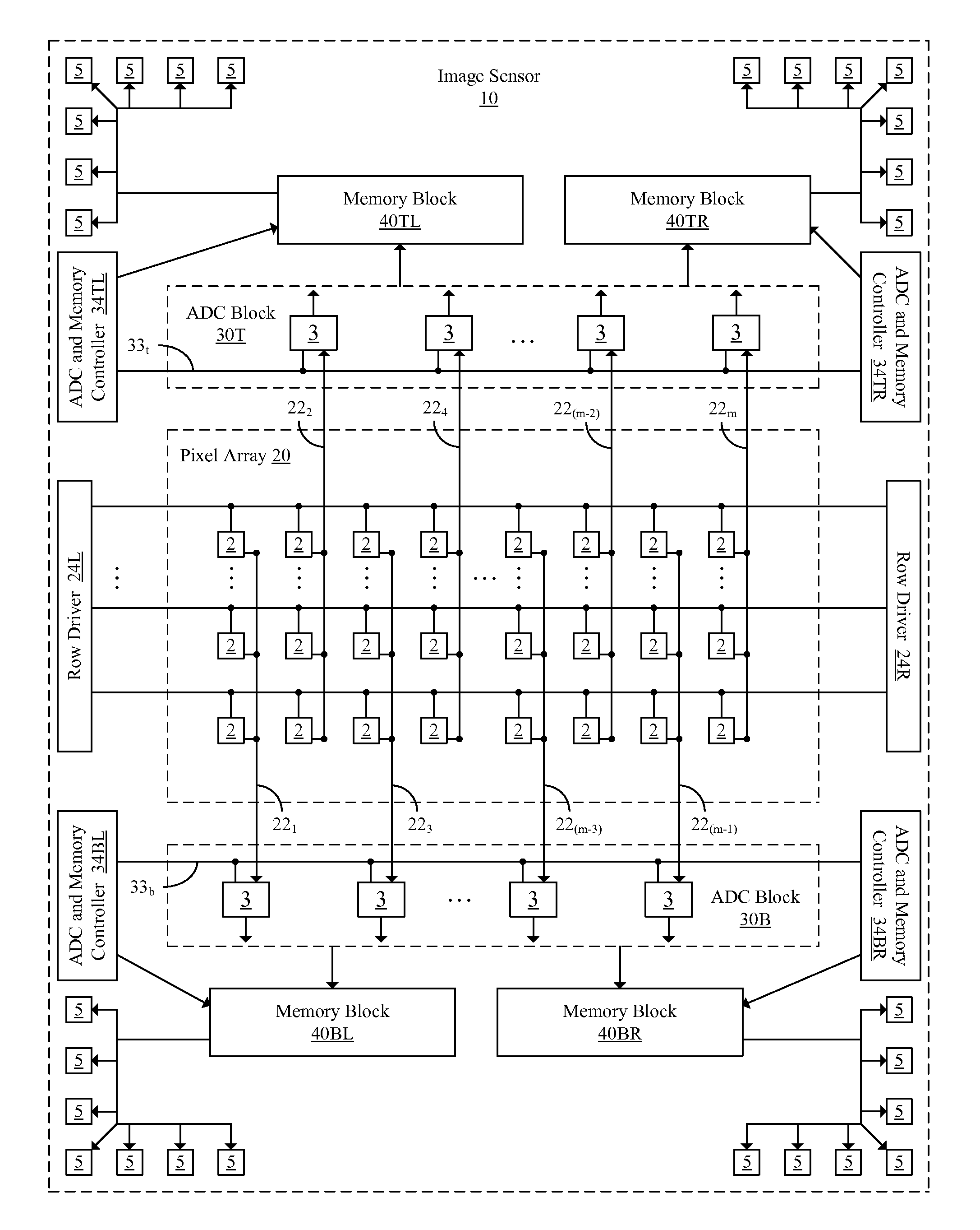
[0067]FIG. 5 illustrates a block diagram of an image sensor 10 in accordance with an embodiment of the present invention. The image sensor 10 includes a pixel array 20, a left row driver 24L, a right row driver 24R, a top analog-to-digital conversion (ADC) block 30T, a bottom ADC block 30B, a top / left memory block 40TL, a top / right memory block 40TR, a bottom / left memory block 40BL, a bottom / right memory block 40BR, a top / left ADC and memory controller 34TL, a top / right ADC and memory controller 34TR, a bottom / left ADC and memory controller 34BL, a bottom / right ADC and memory controller 34BR, and pads 5. In various embodiments, the image sensor 10 may be, for example, a high speed complimentary metal oxide semiconductor (CMOS) image sensor, or the like.

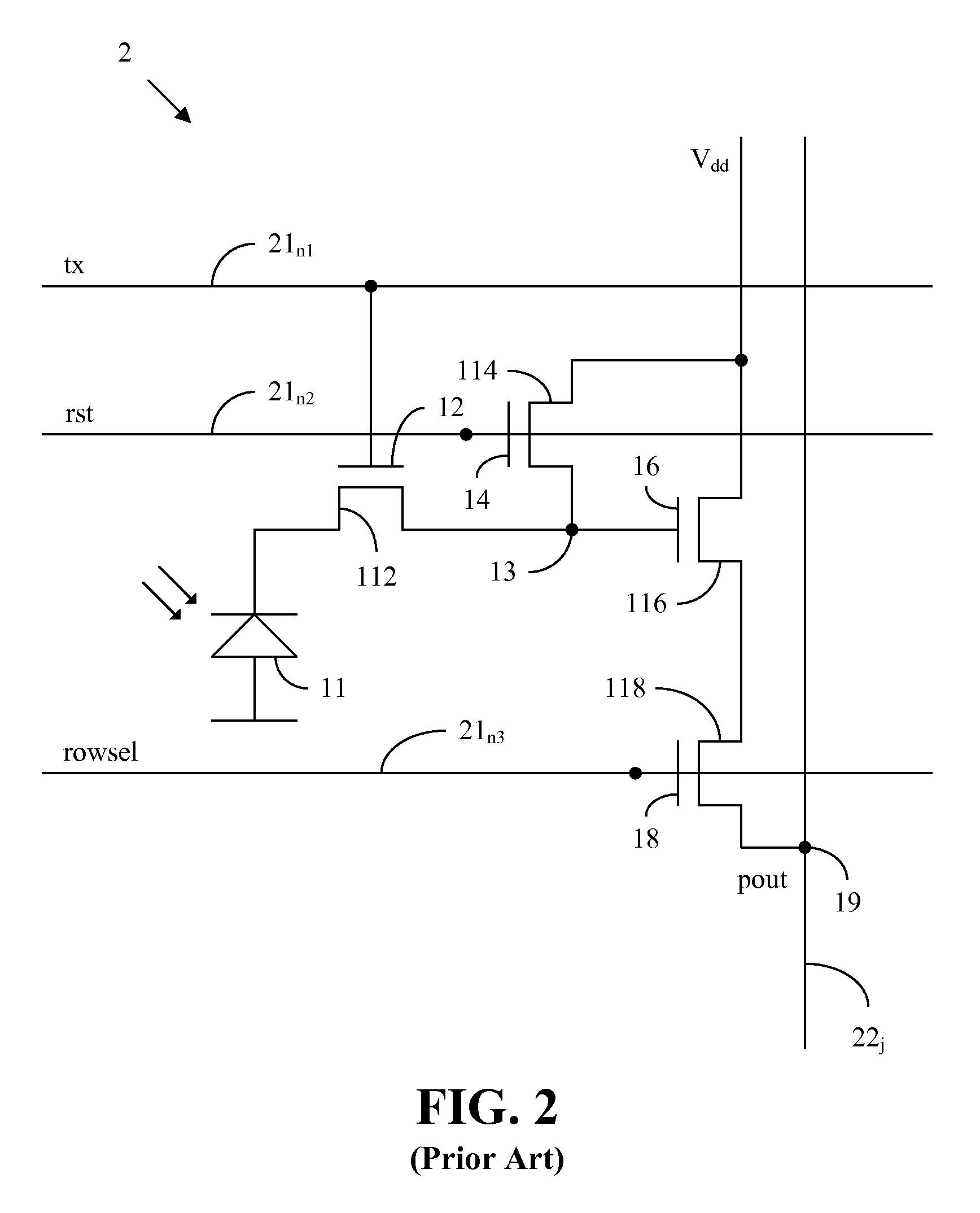
[0068]The pixel array 20 includes a plurality of pixels 2. An example embodiment of the pixel 2 is illustrated in FIG. 2 as a four transistor (4T) pixel. In various embodiments, the pixel 2 may be another type of pixel, such as a thre...


PUM


Abstract

A pipelined readout method in an image sensor includes receiving one or more signals from a pixel of a row of a pixel array into a column storage at least partially during a time that a previously sampled amplified output of the column storage that is based on signals provided by a previous pixel of a previously read out row of the pixel array is converted from analog to digital by an analog-to-digital conversion circuit. The method further includes performing, by the analog-to-digital conversion circuit, analog-to-digital conversion of a sampled amplified output of the column storage that is based on the one or more signals from the pixel at least partially during a time that the column storage receives at least one signal from a another pixel of a subsequently read out row of the pixel array.

Description

[0001]CROSS-REFERENCE TO RELATED PATENT APPLICATIONS[0002]This application is a continuation-in-part of U.S. patent application Ser. No. 12 / 433,711, filed Apr. 30, 2009, which claims the benefit of U.S. Provisional Patent App. Ser. No. 61 / 049,741, filed May 1, 2008, the entire contents of both of which are incorporated by reference herein.BACKGROUND OF THE INVENTION[0003]1. Field of the Invention[0004]Embodiments of the present invention relate generally to image sensors and methods and, in specific embodiments, to image sensors with column readout circuits.[0005]2. Related Art[0006]Image sensors have found wide application in consumer and industrial electronics, and have enabled an explosion in a number of digital cameras and digital video devices used for work and entertainment. In many applications, and especially in industrial applications, there is a constant demand for image sensors with faster processing speed and better image quality. Thus, it is advantageous to develop new ...

Claims


Application Information

Patent Timeline
Patent Type & Authority Applications(United States)
IPC IPC(8): H04N5/335
CPCH04N5/378H04N5/3742H04N25/767H04N25/75
Inventor KRYMSKI, ALEXANDER
Owner KRYMSKI ALEXANDER
Why Eureka
Try Eureka