Bonded wire semiconductor device

Active Publication Date: 2013-02-07
NXP USA INC
View PDF0 Cites 0 Cited by
  • Summary
  • Abstract
  • Description
  • Claims
  • Application Information

AI Technical Summary

Benefits of technology

The present invention is directed to a bonded wire semiconductor device and, more particularly, to a bonded wire semiconductor device with reduced size and complexity of the electrical connections while maintaining the same or greater functionality and complexity of the electronic circuits integrated in the dies. The invention addresses the issue of defects caused by electrical contact between adjacent bond wires caused by different amounts of bond wire sway and sweep during the manufacturing process. The invention provides a solution to reduce the risk of defects by optimizing the distance between the lead fingers and the bond pads on the semiconductor die. The technical effect of the invention is to improve the reliability and efficiency of bonded wire semiconductor devices with reduced size and complexity of the electrical connections.

Problems solved by technology

This aggravates the risk of defects caused by electrical contact between adjacent bond wires.
Bond wire sway and sweep may especially be caused by flow of the molding compound during its injection.

Method used


Image

  • Bonded wire semiconductor device
  • Bonded wire semiconductor device
  • Bonded wire semiconductor device

Examples


Embodiment Construction

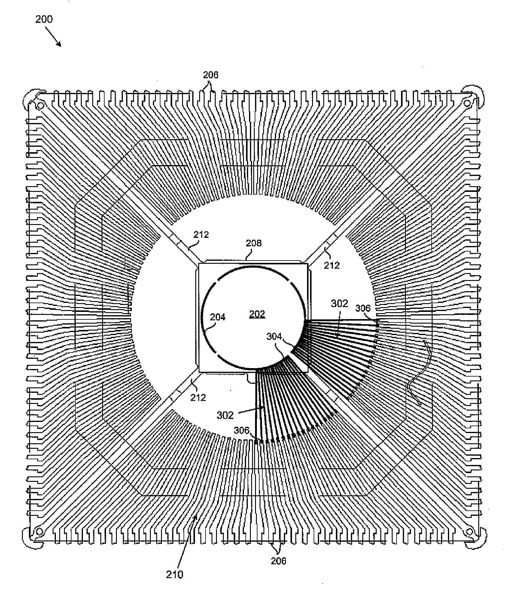
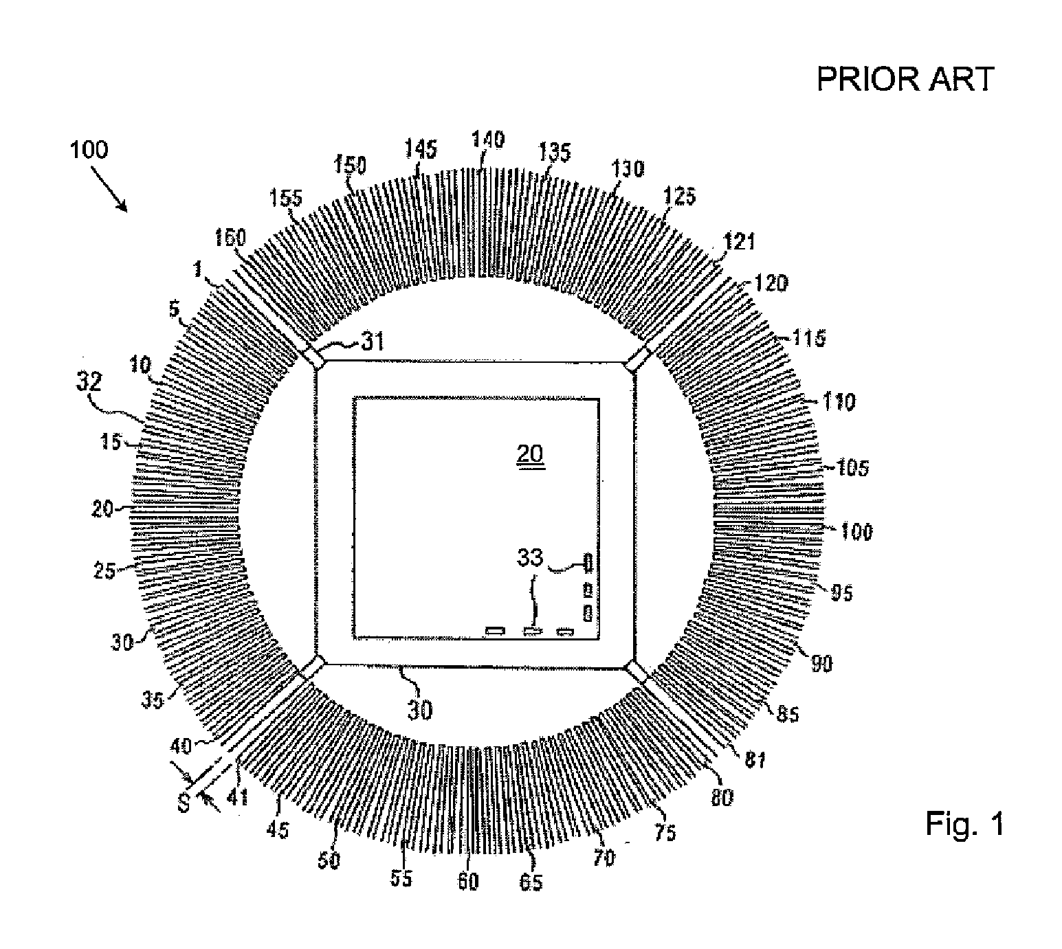
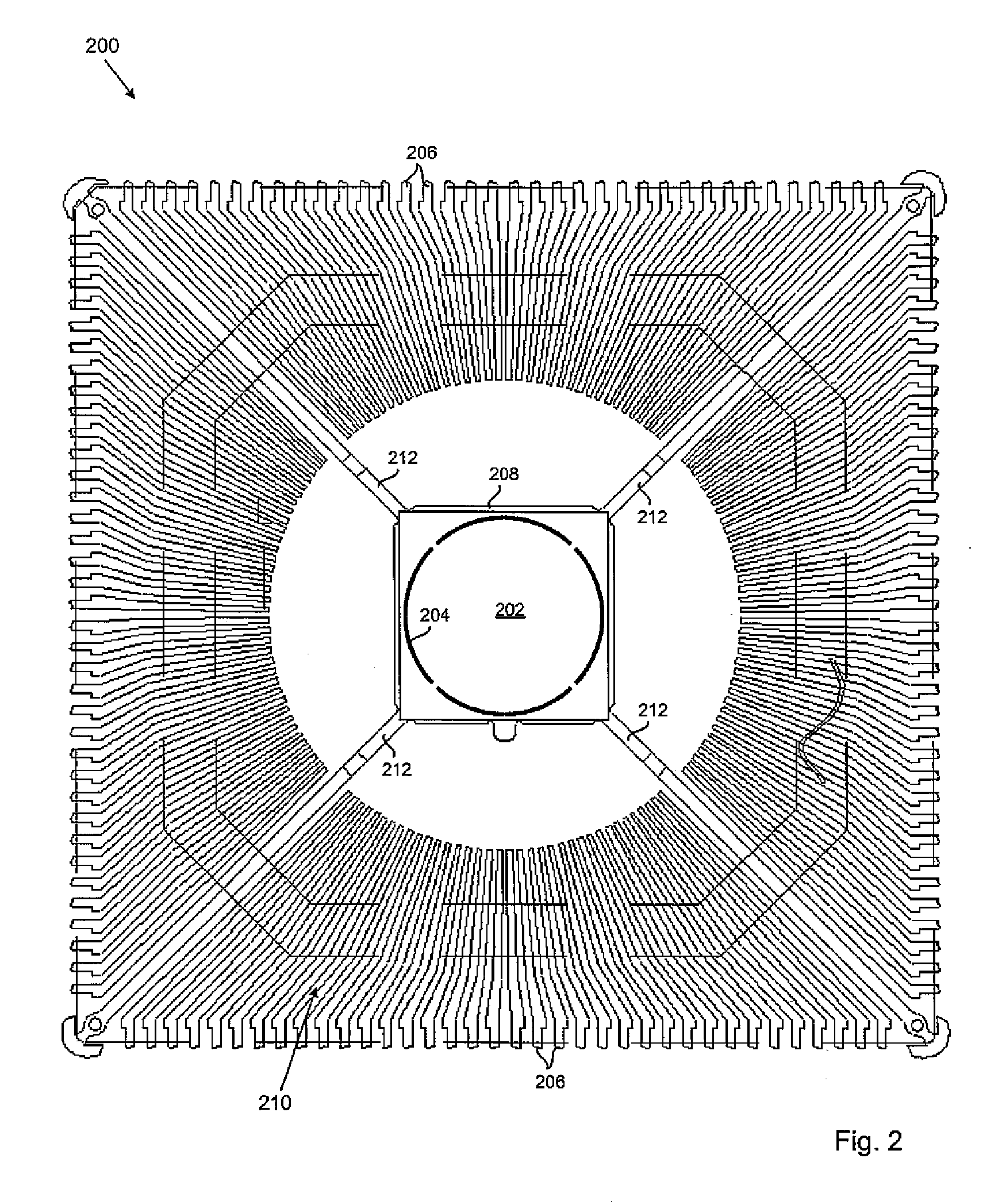
[0011]FIG. 1 shows a sub-assembly 100 in a known bonded wire semiconductor device at an intermediate stage in its manufacture. The sub-assembly 100 comprises a square semiconductor die 20 and a lead frame including a square die pad 30 with tie bars 31 extending from the corners thereof. The lead frame also comprises a plurality of lead fingers 32 (with identification numbers shown from 1 to 160) whose inner ends are arranged in a circular array about the die pad 30. Each of the lead fingers 32 connects to a corresponding bond pad 33 on the semiconductor die 20 with a bond wire (not shown). The bond wires are bonded to the lead fingers 32 at their outer ends and to the bond pads 33 at their inner ends. The lead fingers 32 are arranged in a circular disposition such that the pitch and width of the lead fingers 32 may be relatively constant around the circumference of the lead frame.

[0012]In the sub-assembly 100, the inner ends of the lead fingers 32 are arranged in a circular array wh...


PUM


Abstract

A bonded wire semiconductor device includes a sub-assembly including a semiconductor die having an active face with a set of internal electrical contact elements and an externally exposed set of electrical contact elements. A set of bond wires make respective electrical connections between the internal electrical contact elements and the externally exposed set of electrical contact elements. A molding compound encapsulates the semiconductor die with the active face embedded in the molding compound. The bond wires have the same length. The bond wires are bonded to the internal electrical contact elements and to the externally exposed electrical contact elements at first and second curved arrays and of bond positions respectively. The first and second curved arrays and of bond positions have corresponding concentric shapes.

Description

BACKGROUND OF THE INVENTION[0001]The present invention is directed to semiconductor device packaging and, more particularly, to a bonded wire semiconductor device.[0002]Semiconductor device packaging fulfils basic functions such as providing electric connections and protecting the die against mechanical and environmental stresses. Continued progress in reducing the size of the semiconductor dies and increasing functionality and complexity of the electronic circuits integrated in the dies requires size reduction of the packaging with the same or greater complexity of the electrical connections with external circuits.[0003]Semiconductor devices are commonly packaged for surface mounting by embedding one or more semiconductor dies. Exposed electrical contacts for connection with external circuits are integrated in the package and are connected internally with electrical contact elements such as pads on the semiconductor die. Various techniques are available for connecting the exposed e...

Claims


Application Information

Patent Timeline
IPC IPC(8): H01L23/495
CPCH01L23/4952H01L23/49541H01L2224/48245H01L24/49H01L2224/49173H01L24/48H01L2224/48247H01L2924/181H01L2924/00014H01L2924/00H01L2224/45099H01L2224/05599
Inventor ONG, LI TING CELINAAU, YIN KHENGPOH, ZI-SONG
Owner NXP USA INC
Why Eureka
Try Eureka