Substrate, electronic device, and electronic apparatus

a technology of electronic devices and substrates, applied in the direction of electrical apparatus construction details, instruments, basic electric elements, etc., can solve the problems of cracking beginning at the place of the bonding material (solder) and achieve the effect of high reliability

Active Publication Date: 2013-02-07
SEIKO EPSON CORP
View PDF4 Cites 9 Cited by
  • Summary
  • Abstract
  • Description
  • Claims
  • Application Information

AI Technical Summary

Benefits of technology

[0011]With this configuration, stress can be received by “line” at the circle contacting portion, and stress acting on the boundary between the circle contacting portion and a bonding material can be distributed more extensively. Therefore, in the case of mounting the substrate on a mounting board via a bonding material, it is possible to prevent or suppress the occurrence of a crack in the bonding material due to the stress.Application Example 2
[0035]With this configuration, an electronic apparatus with high reliability is obtained.

Problems solved by technology

However, in the ceramic package of Patent Document 1, since the place indicated by the reference sign M. is a “point”, the stress acts concentratedly on the place, resulting in a problem that a crack beginning at the place occurs in the bonding material (solder).

Method used


Image

  • Substrate, electronic device, and electronic apparatus
  • Substrate, electronic device, and electronic apparatus
  • Substrate, electronic device, and electronic apparatus

Examples


first embodiment

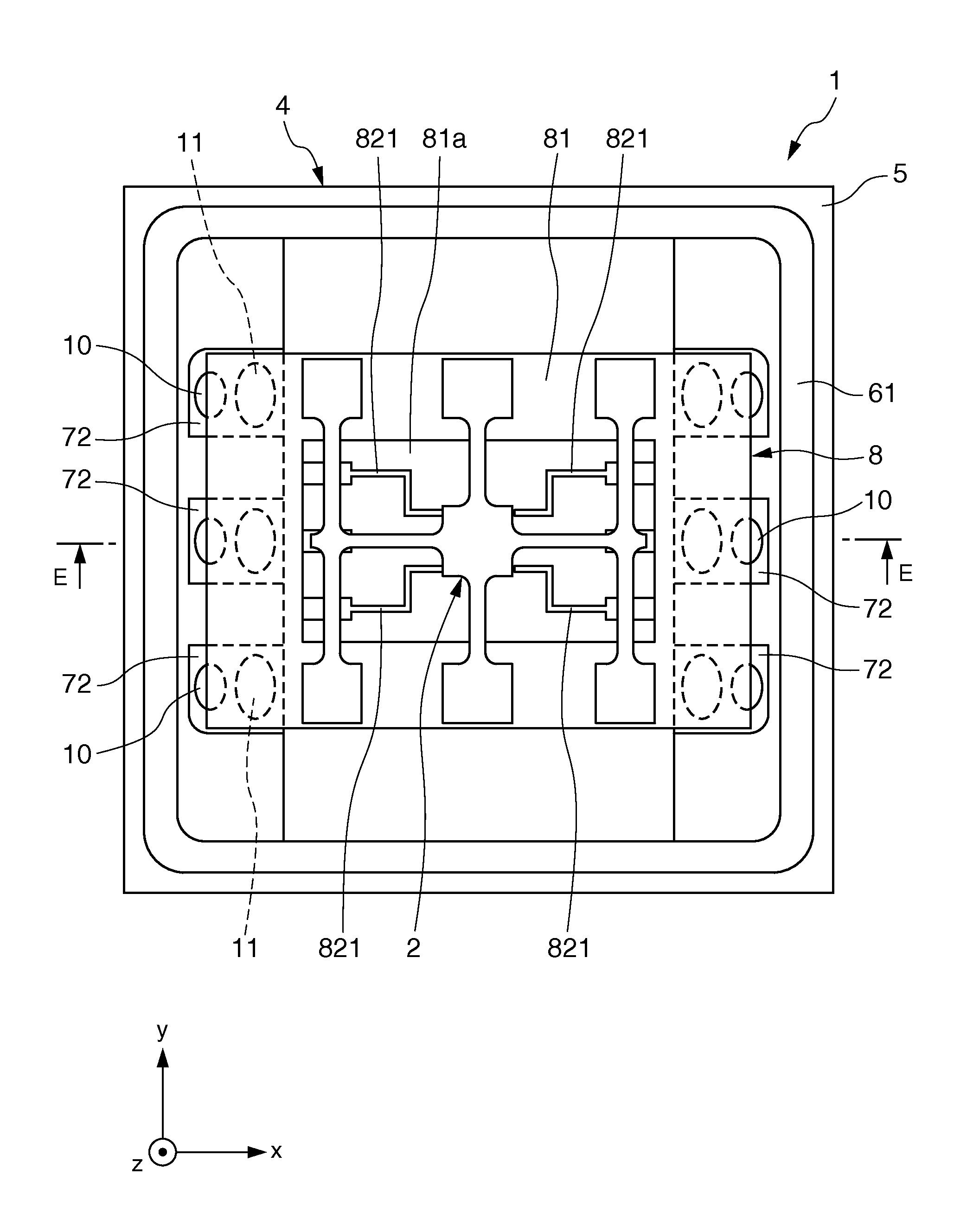
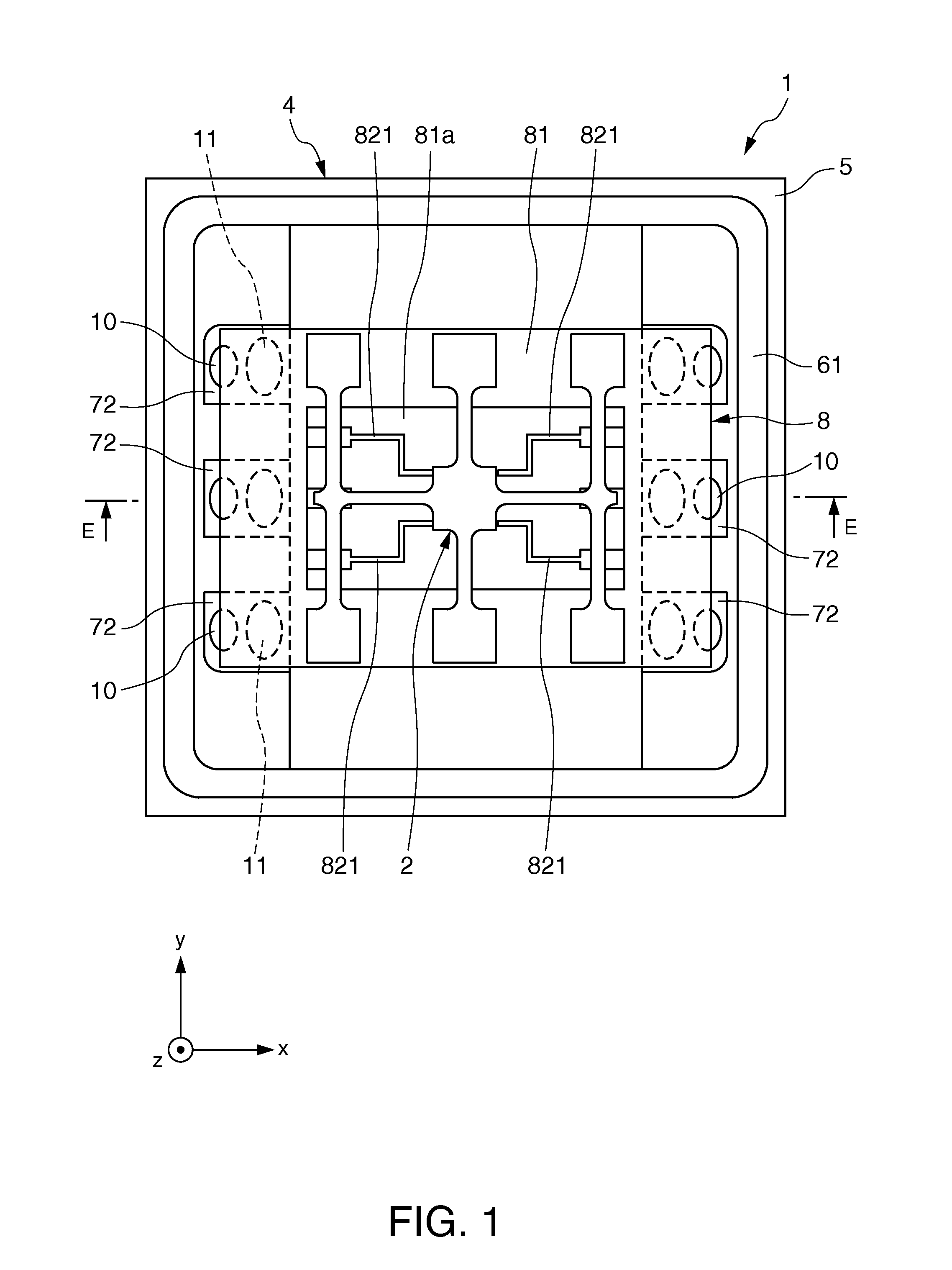
[0049]First, a first embodiment of an electronic device (electronic device according to the invention) incorporating therein a substrate according to the invention will be described.

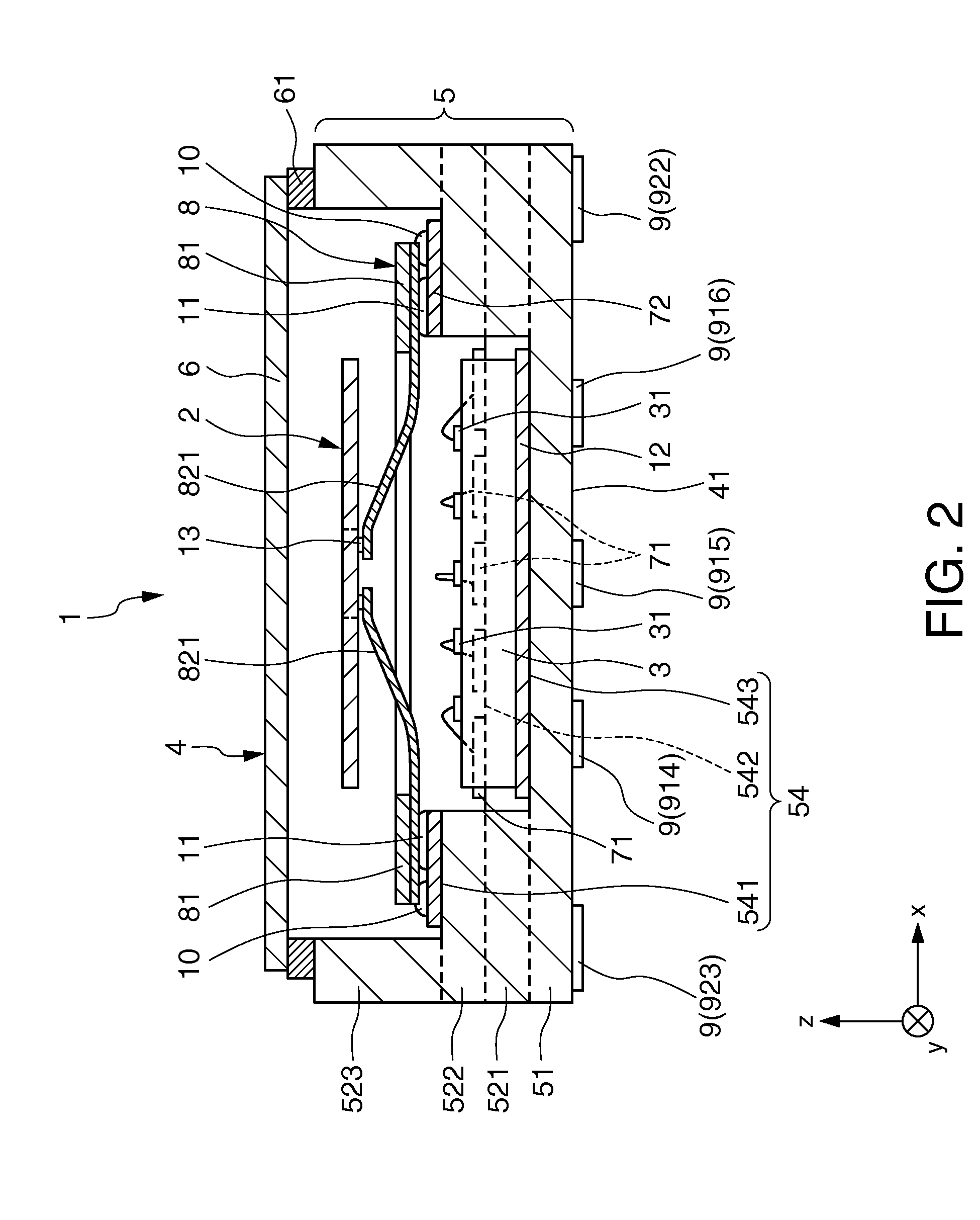
[0050]FIG. 1 is a plan view (top view) showing the first embodiment of the electronic device according to the invention. FIG. 2 is a cross-sectional view taken along line E-E of the electronic device shown in FIG. 1. FIGS. 3A and 3B are plan views of a gyro element of the electronic device shown in FIG. 1. FIGS. 4A and 4B are plan views explaining the driving of the gyro element shown in FIGS. 3A and 3B. FIG. 5 is a plan view showing a supporting substrate of the electronic device shown in FIG. 1. FIG. 6 is a plan view (bottom view) of the electronic device shown in FIG. 1. FIG. 7 is a cross-sectional view showing a state where the electronic device shown in FIG. 1 is mounted on a mounting board. In the following, the front side of the sheet in FIG. 1 is referred to as “upper”, the back side of the sheet...

second embodiment

[0106]Next, a second embodiment of an electronic device of the invention will be described.

[0107]FIG. 8 is a perspective view of the electronic device according to the second embodiment of the invention. FIG. 9 is a cross-sectional view of the electronic device shown in FIG. 8.

[0108]Hereinafter, the electronic device of the second embodiment will be described mainly on the difference from the above-described embodiment. Descriptions of matters similar to those of the above-described embodiment are omitted.

[0109]The electronic device according to the second embodiment of the invention is similar to that of the above-described first embodiment, excepting that the configuration of the circle contacting portion of the sub-electrode terminal is different. Configurations similar to those of the above-described first embodiment are denoted by the same reference and numeral signs.

[0110]In the embodiment, the configurations of the sub-electrode terminals 921 to 924 are similar to each other....

third embodiment

[0116]Next, a third embodiment of an electronic device of the invention will be described.

[0117]FIG. 10 is a plan view (bottom view) of the electronic device according to the third embodiment of the invention.

[0118]Hereinafter, the electronic device of the third embodiment will be described mainly on the difference from the above-described embodiment. Descriptions of matters similar to those of the above-described embodiment are omitted.

[0119]The electronic device according to the third embodiment of the invention is similar to that of the above-described first embodiment, excepting that the configuration of the sub-electrode terminal is different. Configurations similar to those of the above-described first embodiment are denoted by the same reference and numeral signs.

[0120]As shown in FIG. 10, in the electronic device 1 of the embodiment, the sub-electrode terminals 921 and 923 arranged in the y-axis direction are formed integrally with each other, and the sub-electrode terminals...


PUM


Abstract

A substrate includes: a base; and a plurality of bonding terminals arranged on at least one surface of the base, wherein the plurality of bonding terminals include a first bonding terminal and a second bonding terminal, the first bonding terminal and the second bonding terminal include, in plan view of the base, a circle contacting portion extending along the circumference of a circle tangent to the first bonding terminal and the second bonding terminal, all of the plurality of bonding terminals are arranged so as not to protrude from an area including the circle and the inside thereof, and the circle contacting portion includes at least a first circle contacting portion disposed in the first bonding terminal and a second circle contacting portion disposed in the second bonding terminal.

Description

BACKGROUND[0001]1. Technical Field[0002]The present invention relates to a substrate, an electronic device, and an electronic apparatus.[0003]2. Related Art[0004]Heretofore, electronic devices in which a functional element, such as a gyro element, and an IC (Integrated Circuit) chip which performs the driving or the like of the functional element are disposed within a casing have been known. The electronic device has external mounting terminals on a rear surface of the casing, and is mounted on a mounting board via the external mounting terminals (refer to JP-A-2009-99665 (Patent Document 1)).[0005]On a rear surface of a ceramic package of Patent Document 1, main electrode patterns and sub-electrode patterns are formed as external mounting terminals. Mounting of the ceramic package on a mounting board is performed by bonding the main electrode patterns and the sub-electrode patterns with the mounting board via solder.[0006]The mounting board is usually composed of a glass epoxy boar...

Claims


Application Information

Patent Timeline
Patent Type & Authority Applications(United States)
IPC IPC(8): H05K7/02H05K1/11
CPCG01C19/5663H01L23/49838H01L2224/48091H01L2224/73265H01L2924/00014
Inventor SATO, KENJI
Owner SEIKO EPSON CORP
Why Eureka
Try Eureka