LED package device

Active Publication Date: 2013-02-28
ADVANCED OPTOELECTRONICS TECH
View PDF10 Cites 15 Cited by
  • Summary
  • Abstract
  • Description
  • Claims
  • Application Information

AI Technical Summary

Problems solved by technology

Since these LED package devices are applied in a backlight unit or a lighting device, these LED package devices may be assembled in an array or into a light bar unit, whereby hot s

Method used


Image

  • LED package device
  • LED package device
  • LED package device

Examples


Example

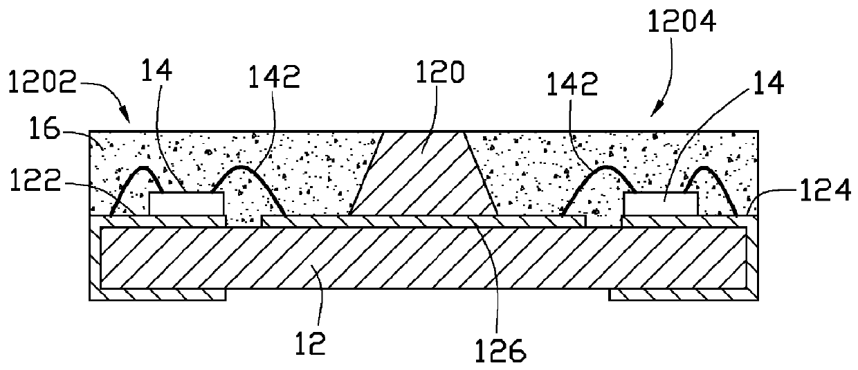
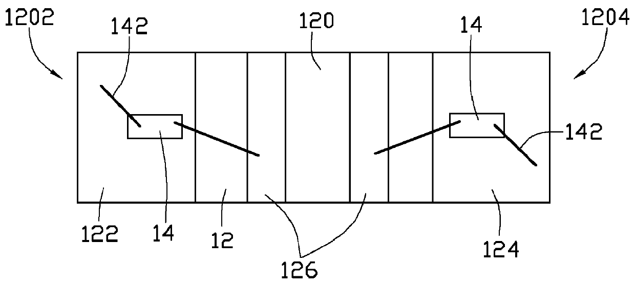
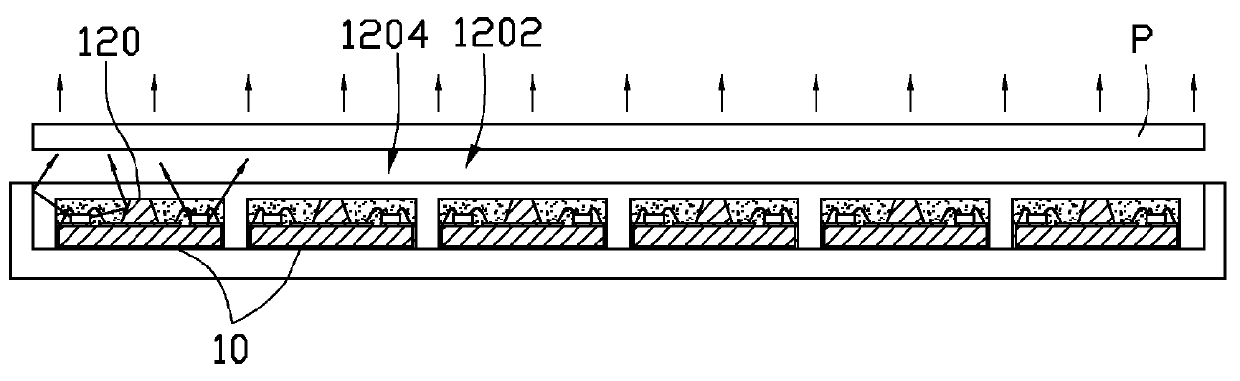
[0009]Referring to FIG. 1, the disclosure provides a first embodiment of an LED package device 10 comprising a substrate 12, two LED dies 14, and an encapsulation layer 16. The substrate 12 includes two regions, a first region 1202 and a second region 1204 both defined on a surface of the substrate 12. In the embodiment, the first region 1202 and the second region 1204 are respectively located on two opposite ends of the substrate 12.

[0010]The substrate 12 comprises a first electrode 122, a second electrode 124, and a dam 120. The first electrode 122 and the second electrode 124 located on the surface of the substrate 12 are used for bonding the two LED dies 14. These two LED dies 14 are electrically connected to the first electrode 122 and the second electrode 124 by conductive wires 142. Alternatively, the LED dies 14 can be electrically connected to the first and second electrodes 122, 124 by flip chip (not shown). In the embodiment, the first electrode 122 and the second electro...

Example

[0015]Referring to FIG. 4 and FIG. 5, the disclosure provides a second embodiment of an LED package device 20, which comprises a substrate 22, two LED dies 24, and an encapsulation layer 26. The substrate 22 includes two regions, a first region 2202 and a second region 2204 both are defined on a surface of the substrate 22. In the embodiment, the first region 2202 and the second region 2204 are respectively located on two opposite ends of the substrate 22.

[0016]The substrate 22 comprises a first electrode 222, a second electrode 224, a first connecting electrode 226, a second connecting electrode 228, and a dam 220. In the embodiment, the first electrode 222 and the second electrode 224 located on the surface of the substrate 22 are used for bonding the two LED dies 24; moreover the two LED dies 24 are electrically connected to the first electrode 222 and the first connecting electrode 226, the second electrode 224 and the second connecting electrode 228 by conductive wires 242. Alt...


PUM


Abstract

An LED package device having a dam located on a substrate is provided, by which two regions are defined on the substrate. Two LED dies are respectively disposed on the two regions and separated by the dam; therefore, the LED package device has an enhanced intensity of the lateral-emitting light and a wide light emitting angle. The LED package devices can be used in backlight units to prevent mura and hot spot issues.

Description

1. TECHNICAL FIELD[0001]The disclosure relates generally to light emitting diode (LED) package devices, and particularly to an LED package device having a wide light emitting angle.2. DESCRIPTION OF THE RELATED ART[0002]Light emitting diodes (LEDs) have low power consumption, high efficiency, quick reaction time, long lifetime and the absence of toxic elements such as mercury during manufacturing. Generally, a reflector is used inside an LED package device to increase the light intensity and render the desired color(s). The reflector is able to collect light emitted from an LED chip and directs the light out of the LED package device in a normal direction, which is directly out of a plan view of the LED package device, whereby an intensity of the light from the LED package device in the normal direction is greater than that in lateral directions. Since these LED package devices are applied in a backlight unit or a lighting device, these LED package devices may be assembled in an arr...

Claims


Application Information

Patent Timeline
IPC IPC(8): H01L33/48
CPCH01L2224/48091H01L2224/48227H01L33/60H01L25/0753H01L33/486H01L2924/00014
Inventor CHANG, CHAO-HSIUNGLIN, HOU-TE
Owner ADVANCED OPTOELECTRONICS TECH
Why Eureka
Try Eureka