
Integrated circuit with face-to-face bonded passive variable resistance memory and method for making the same

a passive variable resistance and integrated circuit technology, applied in the field of integrated circuits, can solve the problems of cost and distance of memory to the place it is needed

Inactive Publication Date: 2013-02-28
ADVANCED MICRO DEVICES INC
View PDF9 Cites 41 Cited by
  • Summary
  • Abstract
  • Description
  • Claims
  • Application Information

AI Technical Summary

Benefits of technology

The patent text describes an integrated circuit with a passive variable resistance memory and a method for making it. The integrated circuit includes two integrated circuit dies that are face-to-face mounted together. The first integrated circuit die includes the passive variable resistance memory, while the second integrated circuit die includes memory control logic. The passive variable resistance memory may be memristors, phase-change memory, or magnetoresistive memory. The integrated circuit may also include processor logic on the second integrated circuit die operatively coupled to the memory control logic. The technical effect of this patent is to provide an improved integrated circuit with passive variable resistance memory that can scale beyond DRAM and flash memory, while maintaining low latency and energy efficiency.

Problems solved by technology

Either implementation, however, has issues with cost and distance of the memory to where it is needed on the processor.

Method used


Image

  • Integrated circuit with face-to-face bonded passive variable resistance memory and method for making the same
  • Integrated circuit with face-to-face bonded passive variable resistance memory and method for making the same
  • Integrated circuit with face-to-face bonded passive variable resistance memory and method for making the same

Examples


Embodiment Construction

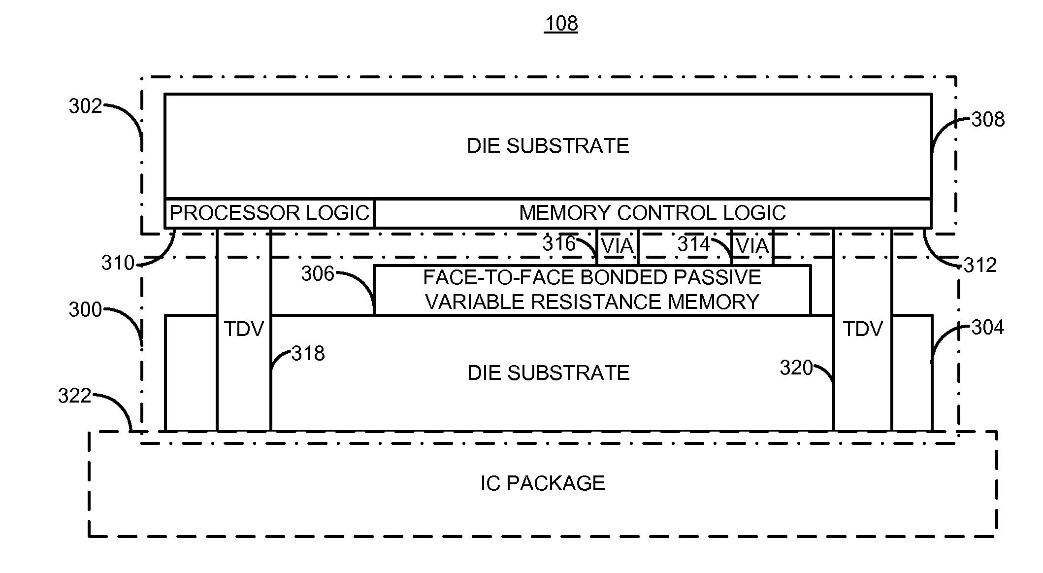
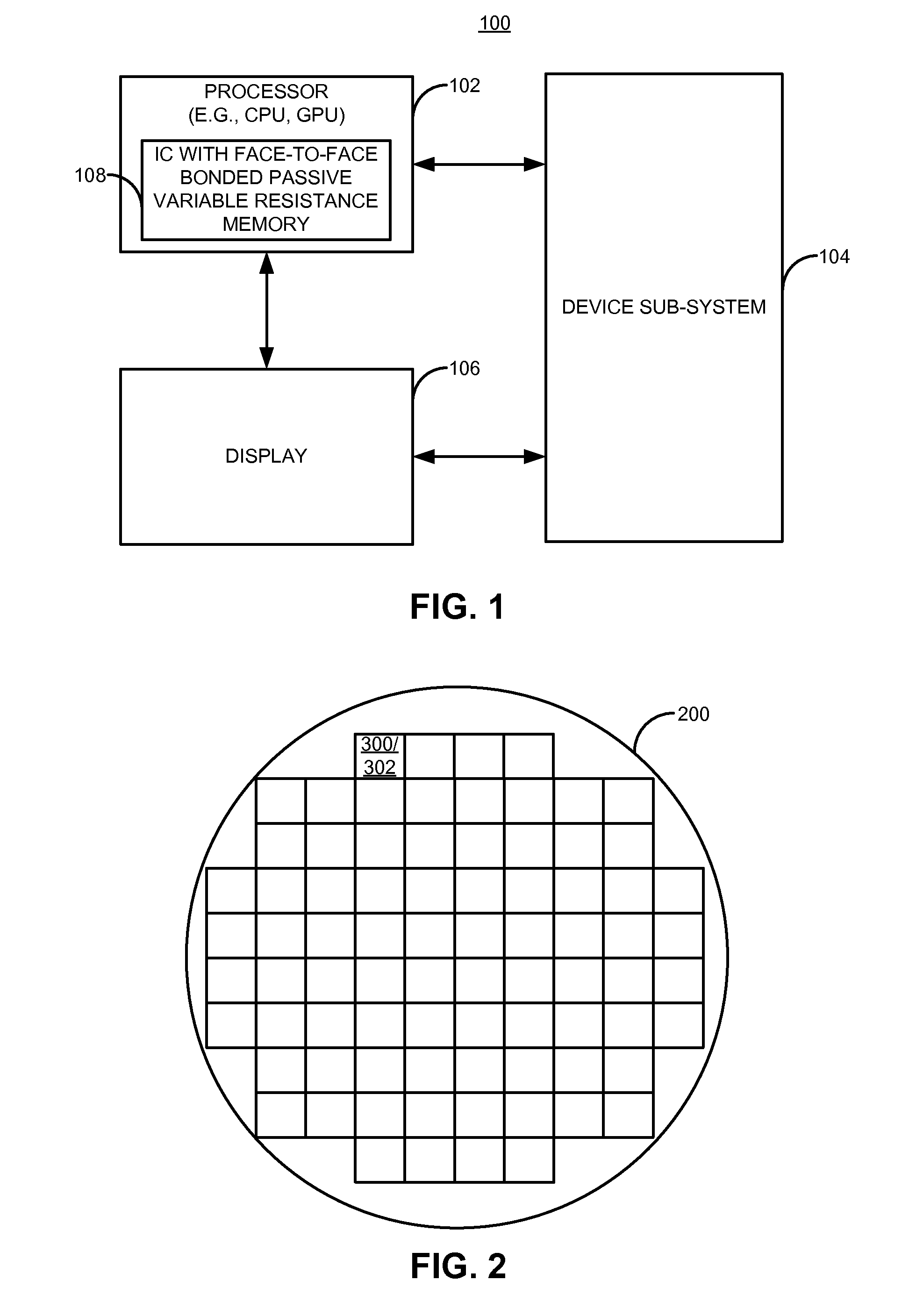
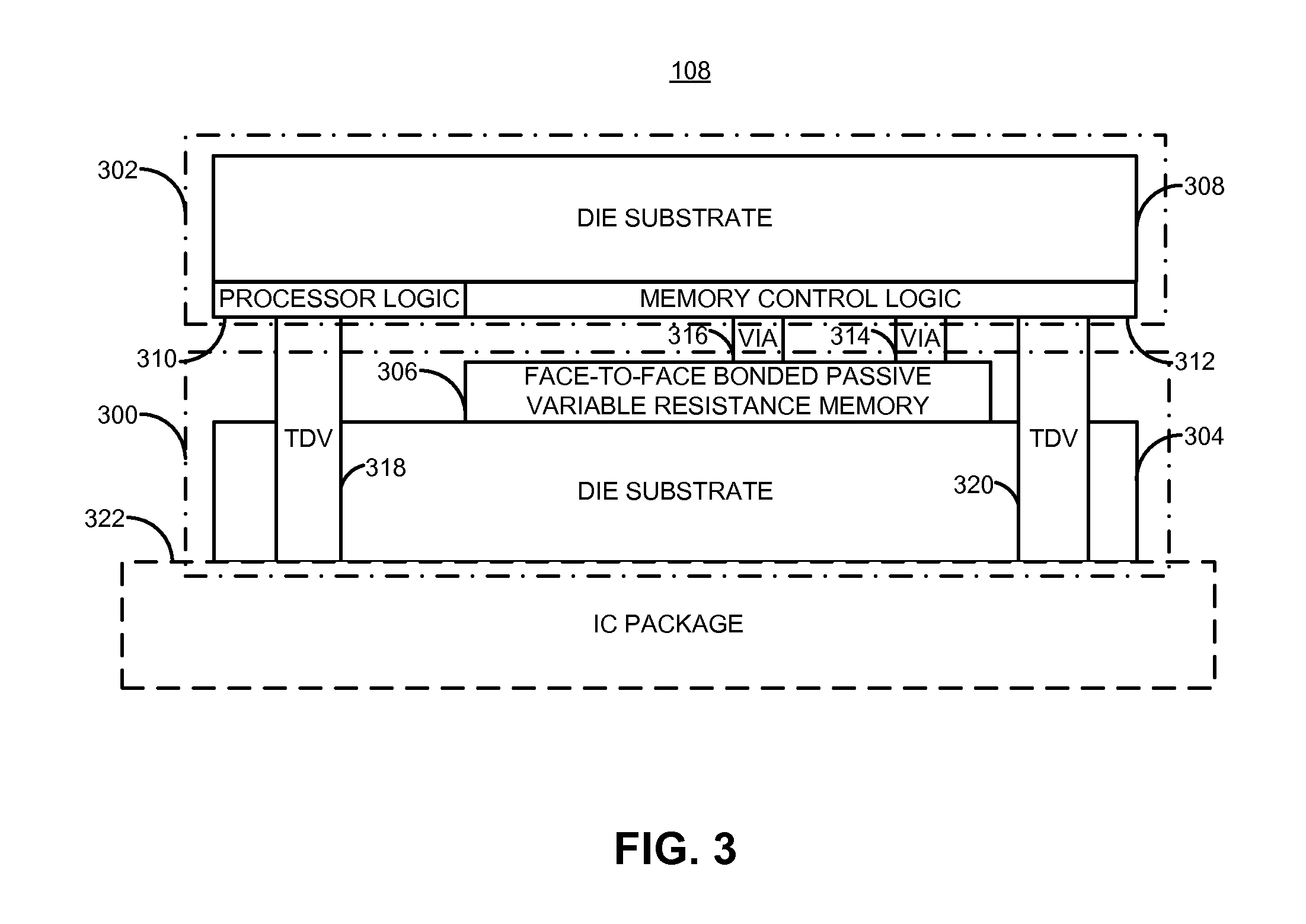
[0015]Briefly, in one example, an integrated circuit includes two integrated circuit dies that are face-to-face mounted together. The first integrated circuit die includes passive variable resistance memory, and the second integrated circuit die includes memory control logic (e.g., CMOS logic circuit). The passive variable resistance memory, also known as resistive non-volatile memory, may be for example memristors, phase-change memory, or magnetoresistive memory. Each memory cell of the passive variable resistance memory on the first integrated circuit die is electrically connected to the memory control logic on the second integrated circuit die through at least one vertical interconnect accesses (vias). For example, the operation (e.g., write / read) of each passive variable resistance memory cell is controlled by the memory control logic. The integrated circuit may also include processor logic on the second integrated circuit die operatively coupled to the memory control logic.

[001...


PUM


Abstract

In one example, an integrated circuit includes two integrated circuit dies that are face-to-face mounted together. The first integrated circuit die includes passive variable resistance memory and the second integrated circuit die includes memory control logic (e.g., CMOS logic circuit). The passive variable resistance memory, also known as resistive non-volatile memory, may be for example memristors, phase-change memory, or magnetoresistive memory. Each memory cell of the passive variable resistance memory on the first integrated circuit die is electrically connected to the memory control logic on the second integrated circuit die through at least one vertical interconnect accesses (vias). For example, the operation (e.g., write / read) of each passive variable resistance memory cell is controlled by the memory control logic. The integrated circuit may also include processor logic on the second integrated circuit die operatively coupled to the memory control logic.

Description

CROSS-REFERENCE TO RELATED APPLICATION[0001]This application is related to co-pending application having docket number 00100.10.0562, filed on even date, having inventors William En et al., titled “INTEGRATED CIRCUIT WITH BACKSIDE PASSIVE VARIABLE RESISTANCE MEMORY AND METHOD FOR MAKING THE SAME”, owned by instant assignee; and co-pending application having docket number 00100.10.0564, filed on even date, having inventors William En et al., titled “INTEGRATED CIRCUIT WITH VERTICALLY INTEGRATED PASSIVE VARIABLE RESISTANCE MEMORY AND METHOD FOR MAKING THE SAME”, owned by instant assignee.BACKGROUND OF THE DISCLOSURE[0002]The disclosure relates generally to an integrated circuit and to a method for making the same.[0003]Dynamic random access memory (DRAM) and flash memory are two dominant memory technologies generally accepted to be nearing the end of their scaling lifetime, and the search is on for a replacement that can scale beyond DRAM and flash memory, while maintaining low latenc...

Claims


Application Information

Patent Timeline
IPC IPC(8): G11C11/56H01L45/00H01L21/50H01L21/62
CPCG11C11/15H01L25/18H01L45/08H01L45/1233H01L45/146G11C13/0011H01L2225/06513H01L2924/0002H01L27/2481G11C13/0004H01L2924/00H10B63/84H10N70/24H10N70/826H10N70/8833
Inventor EN, WILLIAM G.WEISS, DON R.
Owner ADVANCED MICRO DEVICES INC
Learn More