Methods to increase pattern density and release overlay requirement by combining a mask design with special fabrication processes

Inactive Publication Date: 2013-03-14
VIGMA NANOELECTRONICS
View PDF14 Cites 27 Cited by
  • Summary
  • Abstract
  • Description
  • Claims
  • Application Information

AI Technical Summary

Benefits of technology

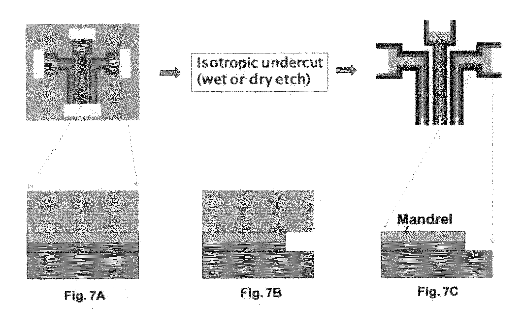
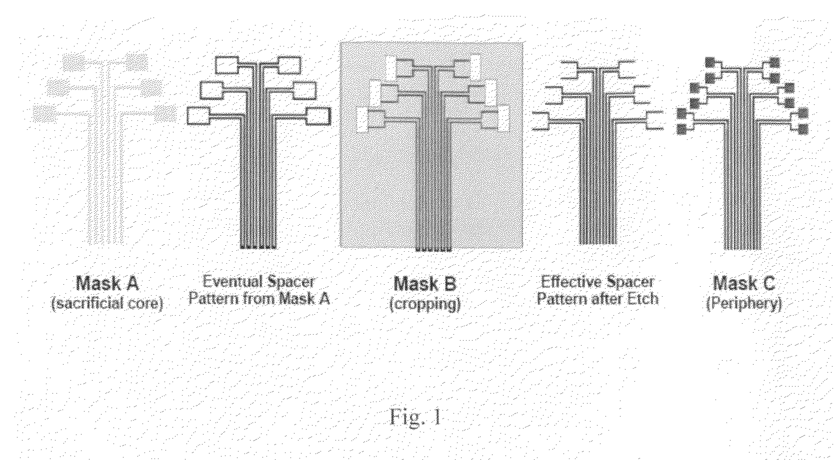
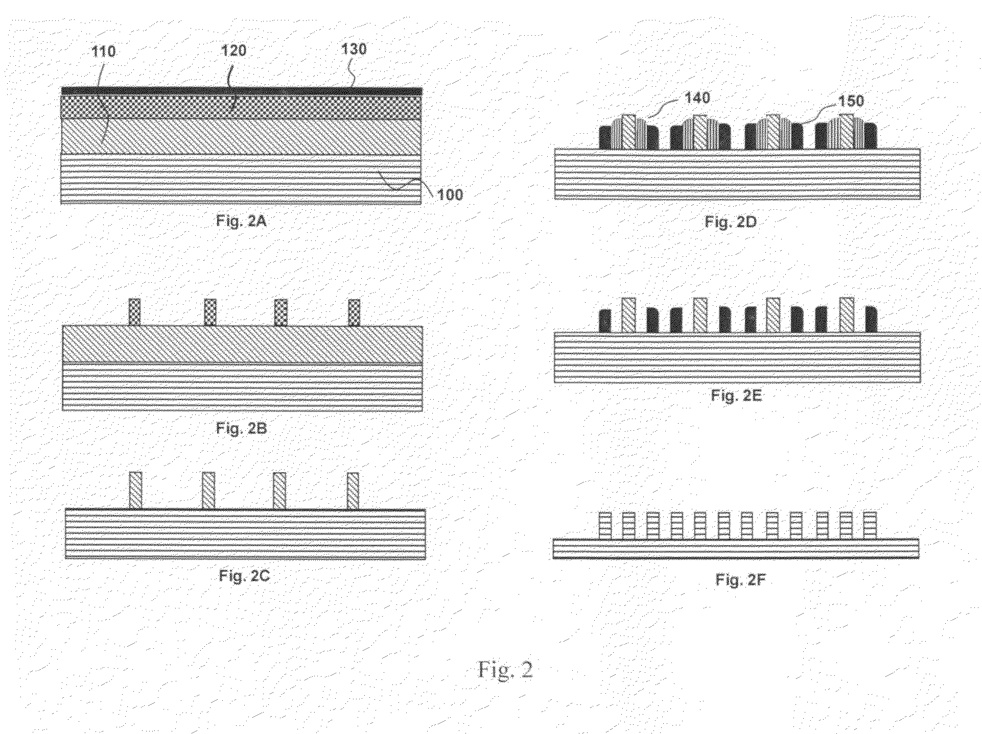
[0005]In a semiconductor process, each critical layer needs to contain both dense arrays (e.g., lines/spaces and pads) and less dense peripheral patterns to perform designed circuit functions. For example, in NAND flash manufacturing wherein the self-aligned double patterning (SADP) process has been widely used, normally the dense arrays and peripheral circuits (including final pads) are decomposed into separate masks and totally 3 masks (sacrificial core mask, cropping/cut mask, and periphery/pad mask) are needed for one critical layer [2]. Unfortunately, the SADP mask design methodology does not work for a SATP process. As shown in FIGS. 2 and 3, stripping sacrificial spacers A will result in a small gap between the mandrel and spacer B. Such a small gap will create severe difficulty in meeting the overlay requirement of the final pad layer since an alignment inaccuracy can easily cause the final pads connected to wrong lines. To release the overlay requirement of a

Problems solved by technology

Unfortunately, the SADP mask design methodology does not work for a SATP process.
As shown in FIGS. 2 and 3, stripping sacrificial spacers A will result in a small gap between the mandrel and space

Method used


Image

  • Methods to increase pattern density and release overlay requirement by combining a mask design with special fabrication processes
  • Methods to increase pattern density and release overlay requirement by combining a mask design with special fabrication processes
  • Methods to increase pattern density and release overlay requirement by combining a mask design with special fabrication processes

Examples


Embodiment Construction

[0016]Embodiments of the present invention pertain to methods of forming patterned features on a substrate having a pitch reduced to one third of what is achievable using standard lithographic techniques. Compared with self-aligned double patterning (SADP) process which has been used in the production of high density 1-D lines / spaces, the invented technique significantly increases the feature density by using a slightly more complex process. While this technique can form bit lines, wider lines and features (e.g., line-end pads, power supply lines, string select lines in NAND devices, etc.) are usually necessary on same layer to form working devices, which requires multiple masks to be used to pattern one critical layer. Therefore, it is important to research a mask design method that not only allows reasonable (i.e., not too tight) overlay specifications, but also requires the minimum number of masks to reduce the process complexity and costs.

[0017]To better understand and appreciat...


PUM


Abstract

A novel process technique and mask design based on the optimized self-aligned triple patterning are invented for the semiconductor manufacturing. This invention pertains to methods of forming one and/or two dimensional features on a substrate having the feature density increased to three times of what is possible using optical lithography, and methods to release the overlay requirement when patterning the critical layers of semiconductor devices.

Description

BACKGROUND OF THE INVENTION[0001]Optical ArF (wavelength: 193 nm) DUV immersion lithography with NA=1.35 can print half-pitch features as small as 38 nm [1]. Self-aligned double patterning (SADP, [2]) has been widely adopted by the memory industry to extend the life of optical lithography, driving the half pitch down to about 19 nm. Sub-19 nm patterning, however, poses tremendous challenges in lithography, materials, and process technologies. EUV, nano-imprint, and e-beam maskless lithography, all with various manufacturability barriers, will not be ready in time for high-volume manufacturing. To meet the scaling timeline, a self-aligned triple patterning (SATP) technology is proposed recently [3, 4], which can potentially drive the resolution of IC features down to about 13 nm when combined with ArF immersion lithography. It was demonstrated that by adding only one extra CVD / spacer step, the SATP process gains 50% improvement in density compared with a SADP process. By designing va...

Claims


Application Information

Patent Timeline
IPC IPC(8): H01L21/311
CPCH01L21/0337H01L21/0338H01L27/1052H01L27/10882H01L27/11573H01L27/11517H01L27/11526H01L27/11563H01L27/10885H10B99/00H10B12/48H10B12/482H10B41/00H10B41/40H10B43/00H10B43/40
Inventor CHEN, YIJIAN
Owner VIGMA NANOELECTRONICS
Why Eureka
Try Eureka