Wavelength variable interference filter, optical filter device, optical module, electronic apparatus, and method of manufacturing the wavelength variable interference filter

a wavelength variable interference and filter technology, applied in the field of wavelength variable interference filters, can solve the problems of difficult bending of the movable section, insufficient bonding strength between the first substrate and the second substrate, and less impact from the outside, so as to achieve accurate parallel relation, improve processing accuracy, and high resolution

Inactive Publication Date: 2013-04-04
SEIKO EPSON CORP
View PDF7 Cites 6 Cited by
  • Summary
  • Abstract
  • Description
  • Claims
  • Application Information

AI Technical Summary

Benefits of technology

[0031]In addition, since the second substrate does not bend, it is possible to accurately maintain a parallel relation between the first reflective film and the second reflective film and extract light having desired wavelength at high resolution.
[0032]Therefore, in the electronic apparatus, when light having target wavelength extracted through light interference by the first reflective film and the second reflective film is detected and various kinds of processing is carried out on the basis of an amount of the light, it is possible to carry out the various kinds of processing on the basis of an accurate light amount and improve processing accuracy.
[0033]Still yet another aspect of the invention is directed to a method of manufacturing a wavelength variable interference filter including: a first substrate; a second substrate opposed to the first substrate; a first reflective film provided on the first substrate; a second reflective film provided on the second substrate and opposed to the first reflective film via an inter-reflective film gap; and a bonding section configured to bond the first substrate and the second substrate, the second substrate including: a movable section on which the second reflective film is provided; a holding section provided on the outer circumferential side of the movable section in plan view of the second substrate viewed from the substrate thickness direction and configured to hold the movable section to be capable of advancing and retracing with respect to the first substrate; and a substrate outer circumferential section provided on the outer circumferential side of the holding section in the plan view, the method including: machining the first substrate to form the first reflective film on the first substrate; machining the second substrate to form the second reflective film on the second substrate; and bonding the first substrate and the second substrate. The forming the second reflective film includes forming, with etching, the holding section including: a flat section having a uniform thickness dimension, which is smaller than thickness dimensions of the movable section and the substrate outer circumferential section; and a holding outer circumferential section provided on the outer circumferential side of the flat section in the plan view of the second substrate viewed from the substrate thickness direction, a thickness dimension of the holding outer circumferential section increasing from the flat section toward the substrate outer circumferential section, and the outer circumferential edge of the holding outer circumferential section being located on the outer side of the inner circumferential edge of the bonding section. The bonding the first substrate and the second substrate includes performing alignment adjustment to locate the inner circumferential edge of the bonding section further on the inner side than the outer circumferential edge of the holding outer circumferential section in plan view of the first substrate and the second substrate viewed from the substrate thickness direction and then pressurizing and bonding the first substrate and the second substrate via the bonding section. In the forming the second reflective film, the second substrate is etched to form the holding section such that the outer circumferential edge of the holding outer circumferential section of the holding section is further on the outer side than the inner circumferential edge of the bonding section. In the bonding section, after the alignment adjustment is performed such that the outer circumferential edge of the holding outer circumferential section of the holding section is on the outer side of the inner circumferential edge of the bonding section, the first substrate and the second substrate are bonded by pressurizing and bonding. By carrying out such pressurizing and bonding, it is possible to firmly bond the first substrate and the second substrate. In the pressurizing and bonding, a load is applied in a direction in which in bonding places (bonding sections) of the first substrate and the second substrate are bonded to each other. Therefore, moment force of bending toward the first substrate is generated in the holding outer circumferential section of the holding section. In this aspect of the invention, the outer circumferential edge of the holding outer circumferential section is located further on the outer side than the inner circumferential edge of the bonding section. A part of the holding outer circumferential section and the bonding section overlap in the filter plan view. Therefore, even if the holding outer circumferential section overlapping the bonding section in the filter plan view receives moment force, the holding outer circumferential section does not bend to the first substrate side because the bonding section is present right under the holding outer circumferential section. Consequently, it is possible to reduce a bend of the second substrate during bonding and prevent contact of the reflective films.

Problems solved by technology

Therefore, if the entire flat section is bonded to the bonding section, it is difficult to bend the movable section.
However, if an area of the bonding section is small, bonding strength of the first substrate and the second substrate cannot be sufficiently increased.
Since the wavelength variable interference filter is housed in the housing, impact from the outside is less easily transmitted to the wavelength variable interference filter.

Method used


Image

  • Wavelength variable interference filter, optical filter device, optical module, electronic apparatus, and method of manufacturing the wavelength variable interference filter
  • Wavelength variable interference filter, optical filter device, optical module, electronic apparatus, and method of manufacturing the wavelength variable interference filter
  • Wavelength variable interference filter, optical filter device, optical module, electronic apparatus, and method of manufacturing the wavelength variable interference filter

Examples


first embodiment

[0051]A first embodiment of the invention is explained below with reference to the accompanying drawings.

1. Schematic Configuration of a Colorimetric Apparatus

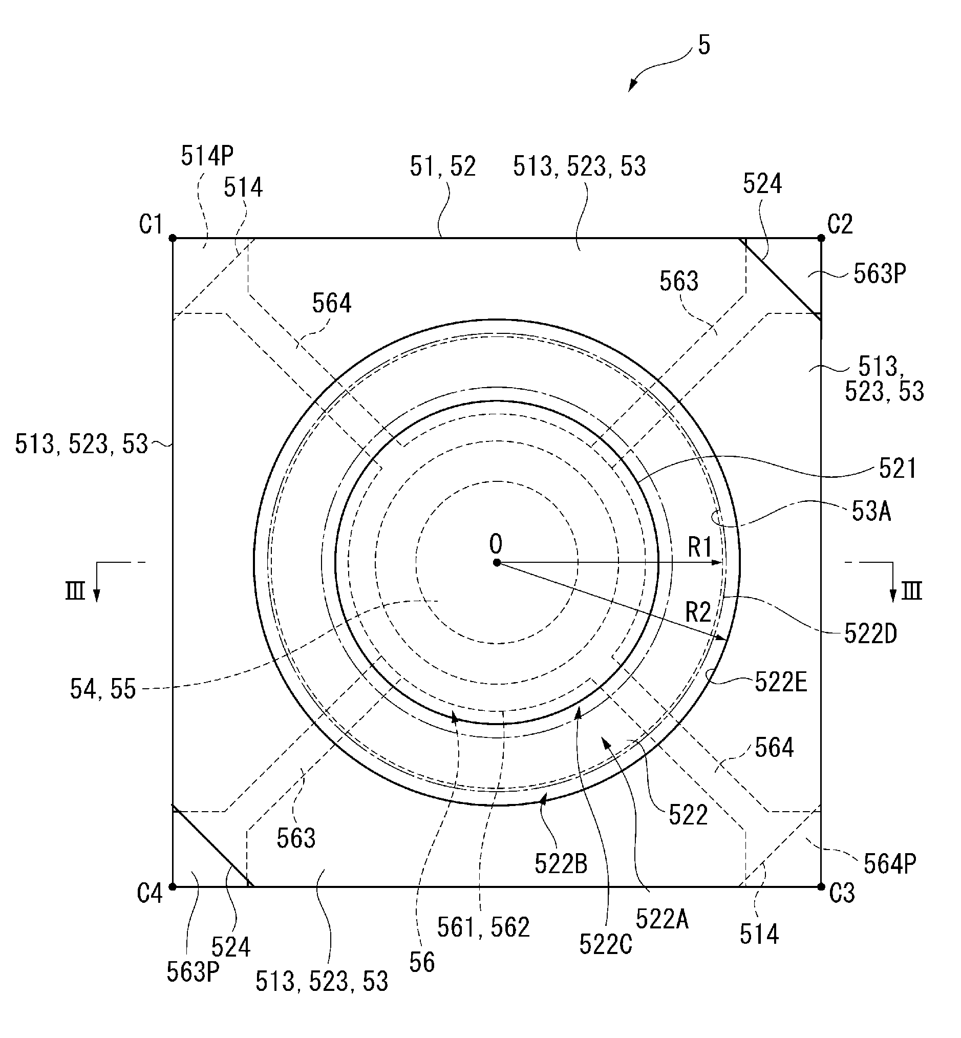
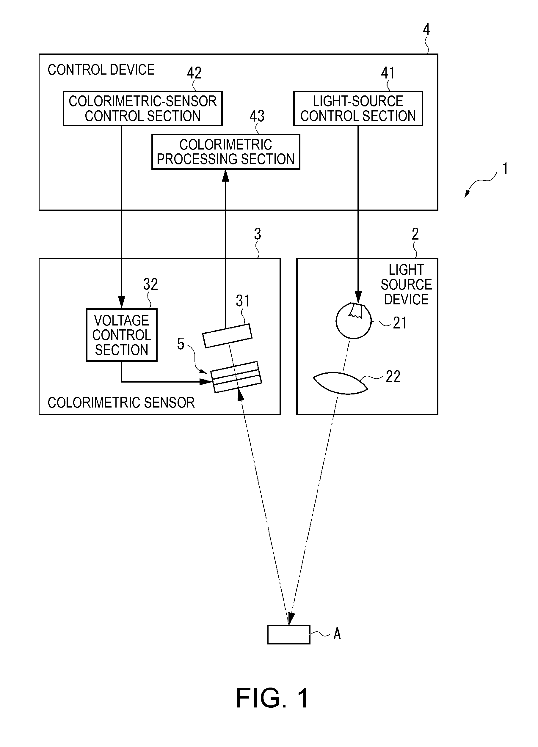
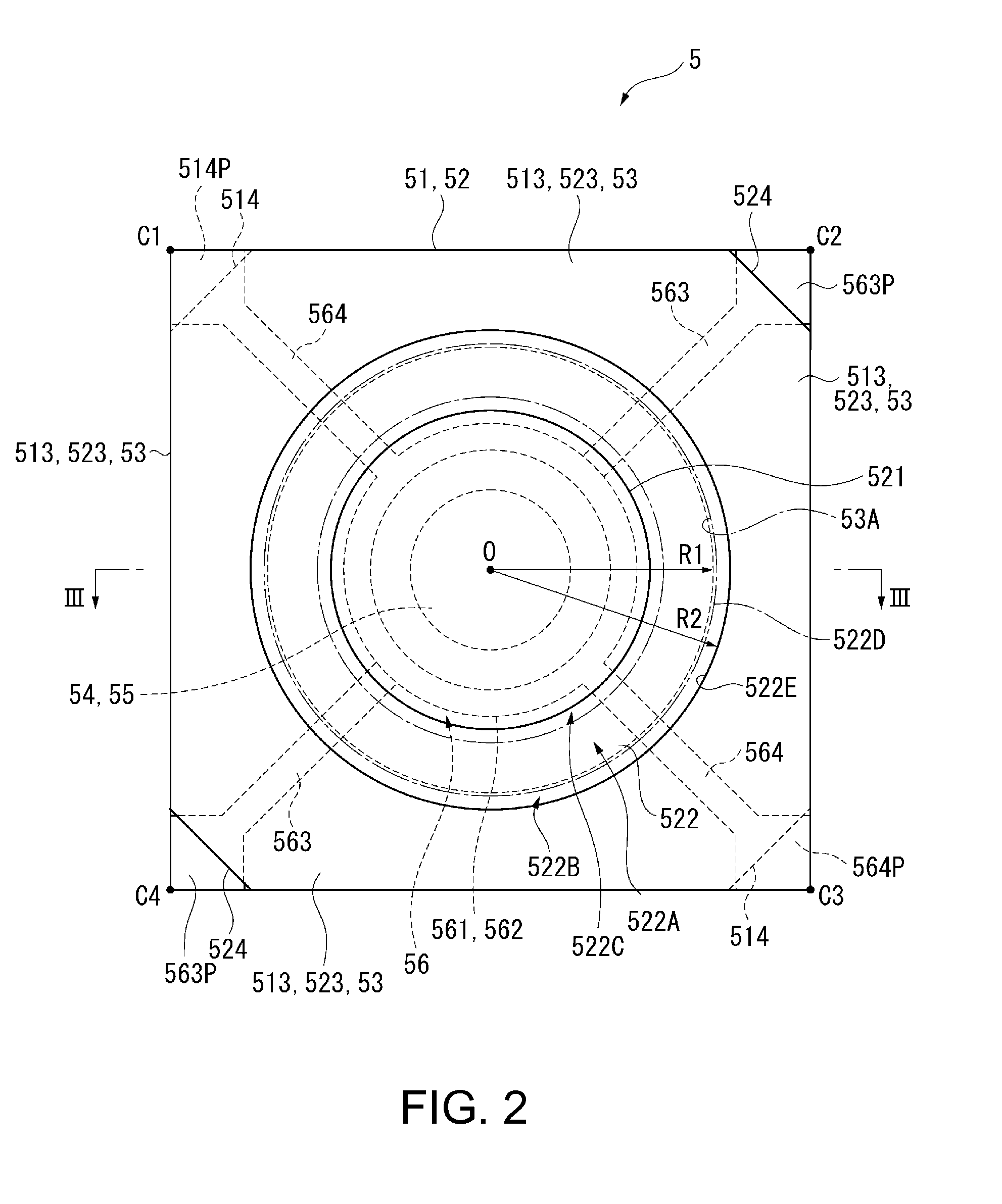
[0052]FIG. 1 is a block diagram of a schematic configuration of a colorimetric apparatus 1 (an electronic apparatus) according to this embodiment.

[0053]The colorimetric apparatus 1 includes, as shown in FIG. 1, a light source device 2 that emits light to an inspection target A, a colorimetric sensor 3 (an optical module), and a control device 4 that controls an overall operation of the colorimetric apparatus 1. The colorimetric apparatus 1 is an apparatus that reflects the light emitted from the light source device 2 on the inspection target A, receives reflected inspection target light in the colorimetric sensor 3, and analyzes and measures the chromaticity of the inspection target light, i.e., a color of the inspection target A on the basis of a detection signal output from the colorimetric sensor 3.

2. Configuration of the L...

second embodiment

[0120]A second embodiment of the invention is explained with reference to the accompanying drawings.

[0121]In the colorimetric apparatus 1 according to the first embodiment, the wavelength variable interference filter 5 is directly provided in the colorimetric sensor 3, which is the optical module. In this case, the wavelength variable interference filter 5 is provided in a predetermined arrangement position provided in the colorimetric sensor 3. Wiring is carried out for the fixed electrode pads 563P and the movable electrode pads 564P. However, some optical module has a complicated configuration. In particular, it is sometimes difficult to directly provide the wavelength variable interference filter 5 in a small optical module. In this embodiment, an optical filter device that enables the wavelength variable interference filter 5 to be easily set even in such an optical module is explained below.

[0122]FIG. 11 is a sectional view showing a schematic configuration of the optical filt...


PUM

PropertyMeasurementUnit
thicknessaaaaaaaaaa
curvature radiusaaaaaaaaaa
thicknessaaaaaaaaaa

Abstract

A wavelength variable interference filter includes a fixed substrate including a fixed reflective film, a movable substrate including a movable reflective film, and a bonding section configured to bond the fixed substrate and the movable substrate. The movable substrate includes a movable section, a holding section, and a substrate outer circumferential section. The holding section includes a flat section having a uniform thickness dimension and a curved surface section provided on the outer circumferential side of the flat section, a thickness dimension of the curved surface section increasing toward the substrate outer circumferential section. The bonding section is provided in an outer circumferential region extending along substrate outer circumferential edges on surfaces opposed to each other of the fixed substrate and the movable substrate. The inner circumferential edge of the bonding section is provided further on the inner side than the outer circumferential edge of the curved surface section.

Description

BACKGROUND[0001]1. Technical Field[0002]The present invention relates to a wavelength variable interference filter for extracting light having specific wavelength from incident light, an optical filter device, an optical module, an electronic apparatus, and a method of manufacturing the wavelength variable interference filter.[0003]2. Related Art[0004]In the past, there is known a wavelength variable interference filter in which reflective films are respectively arranged to be opposed to each other via a predetermined gap on surfaces opposed to each other of a pair of substrates (see, for example, JP-A-2010-8644 (Patent Literature 1)).[0005]In an optical filter (the wavelength variable interference filter) described in Patent Literature 1, a first substrate and a second substrate are bonded and mirrors (reflective films) are respectively provided on surfaces opposed to each other of the substrates. In the wavelength variable interference filter, a groove section having an annular sh...

Claims


Application Information

Patent Timeline
Patent Type & Authority Applications(United States)
IPC IPC(8): G02B5/28B32B37/10
CPCG01J3/26G02B26/001G01N21/65G01J3/50G01N21/359A61B5/1455
Inventor NISHIMURA, TERUYUKIMATSUNO, YASUSHI
Owner SEIKO EPSON CORP
Why Eureka
Try Eureka