Supercharge Your Innovation With Domain-Expert AI Agents!

Nonvolatile Memory Device

a nonvolatile memory and memory device technology, applied in the direction of semiconductor devices, basic electric elements, electrical appliances, etc., can solve the problems of increasing the probability of failure of the high degree of integration, the loss of the isolation structure, and the inability to fully integrate the device, so as to achieve the effect of removing the unnecessary region of the dielectric layer

Inactive Publication Date: 2013-04-11
SK HYNIX INC
View PDF0 Cites 0 Cited by
  • Summary
  • Abstract
  • Description
  • Claims
  • Application Information

AI Technical Summary

Benefits of technology

This approach effectively removes unnecessary dielectric regions without losing EFH, preventing electrical bridges and improving device reliability by ensuring proper gate pattern formation and maintaining the integrity of the isolation structure, thus reducing failure rates.

Problems solved by technology

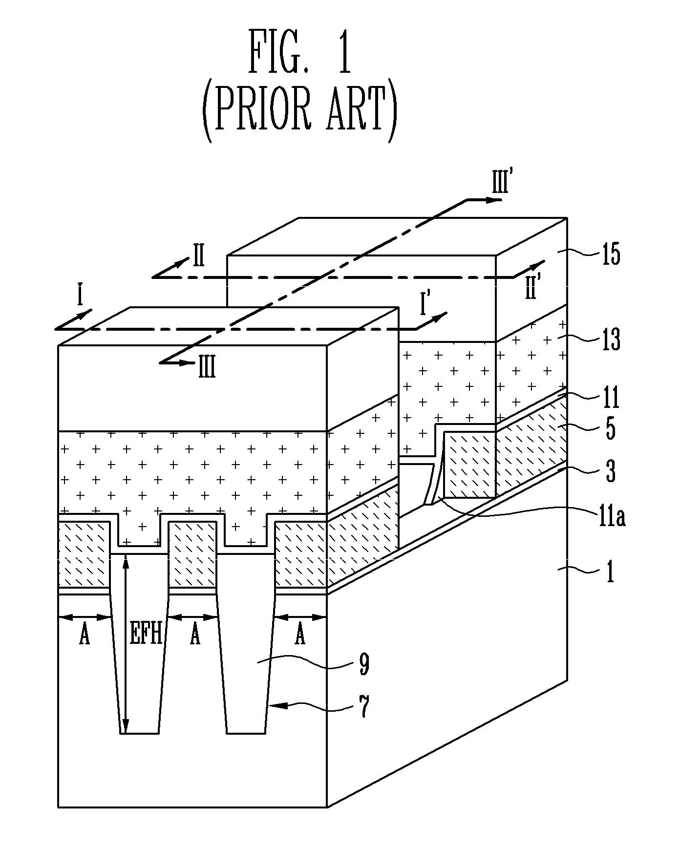
In particular, a NAND flash memory device having a structure advantageous to a high degree of integration is increasingly likely to have failures in a process of forming gate patterns.
In this case, however, the isolation insulation layers 9 are excessively etched, and thus the EFH of the isolation structure may be lost.
The loss of the EFH causes reduction in reliability of the device.

Method used


Image

  • Nonvolatile Memory Device
  • Nonvolatile Memory Device
  • Nonvolatile Memory Device

Examples


Embodiment Construction

[0032]Hereinafter, some exemplary embodiments of the disclosure are described in detail with reference to the accompanying drawings. The drawing figures are provided to allow those having ordinary skill in the art to understand the scope of the embodiments of the disclosure.

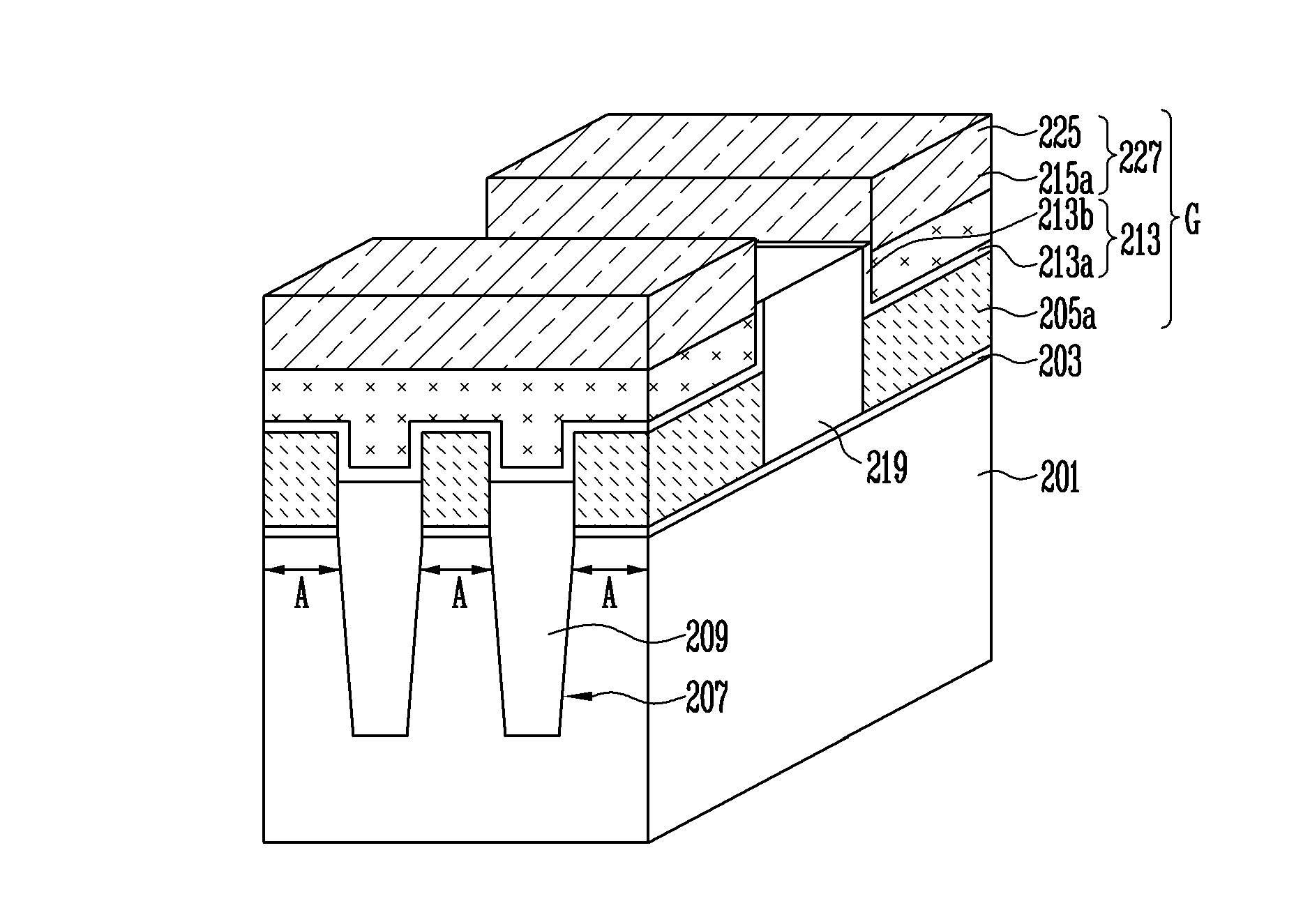
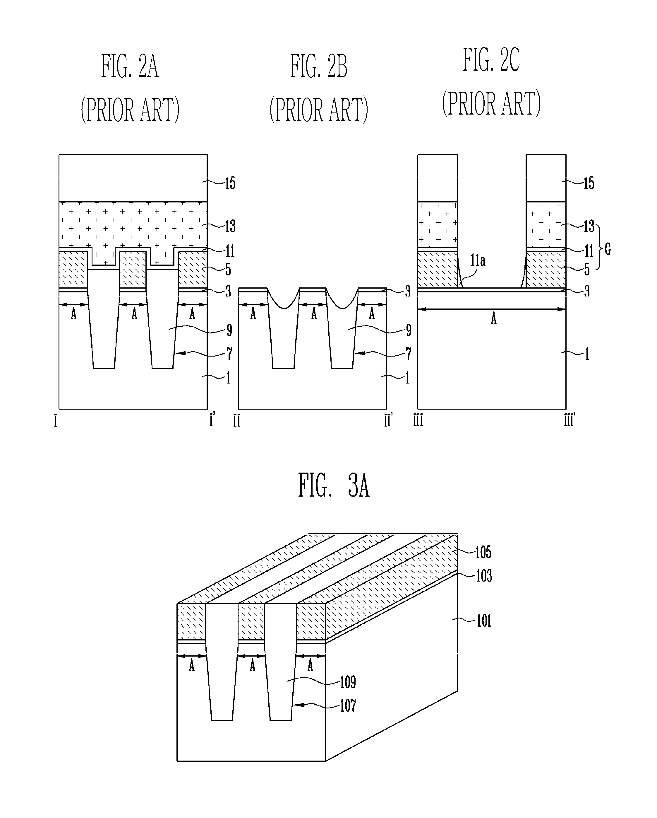
[0033]FIGS. 3A to 3J are depictions illustrating the patterns of a nonvolatile memory device and a method of forming the same according to a first exemplary embodiment of this disclosure. In particular, FIGS. 3A to 3J illustrate the gate patterns of a NAND flash memory device and a method of forming the same.

[0034]Referring to FIG. 3A, an active regions A are defined extending in a longitudinal direction. A semiconductor substrate 101 in which a isolation structure is formed between the active regions A, and a tunnel insulating layer 103 and a charge trap layer 105 are stacked over the active regions A is provided.

[0035]The semiconductor substrate 101 may be formed through the following process.

[0036]First, a wel...


PUM


Abstract

Patterns of a nonvolatile memory device include a semiconductor substrate that defines active regions extending in a longitudinal direction, an isolation structure formed between the active regions, a tunnel insulating layer formed on the active regions, a charge trap layer formed on the tunnel insulating layer, a first dielectric layer formed on the charge trap layer and the isolation structure, wherein the first dielectric layers is extended along a lateral direction, a control gate layer formed on the first dielectric layer, wherein the control gate layer is extended along the lateral direction, and a second dielectric layer formed on a sidewall of the control gate layer along the lateral direction and coupled to the first dielectric layer.

Description

CROSS-REFERENCE TO RELATED APPLICATION[0001]This is a division of U.S. application Ser. No. 13 / 028,364 filed Feb. 16, 2011, which claims the priority benefit under Korean patent application number 10-2010-0014120 filed Feb. 17, 2010, the entire respective disclosures of which are incorporated herein by reference.BACKGROUND[0002]Exemplary embodiments relate generally to the patterns of a nonvolatile memory device and a method of forming the same and, more particularly, to the patterns of a nonvolatile memory device and a method of forming the same, which are capable of improving the failure rate of the device.[0003]In line with an increase in the degree of integration of nonvolatile memory devices and a reduction of the pitch between memory cells, the proportion of defective devices produced in a process of forming patterns constituting a nonvolatile memory device has increased. In particular, a NAND flash memory device having a structure advantageous to a high degree of integration ...

Claims


Application Information

Patent Timeline
Patent Type & Authority Applications(United States)
IPC IPC(8): H01L29/792H10B69/00
CPCH01L27/11568H01L29/792H01L29/66833H10B43/30H01L29/7926
Inventor LEE, YUN KYOUNG
Owner SK HYNIX INC
Features
  • R&D
  • Intellectual Property
  • Life Sciences
  • Materials
  • Tech Scout
  • Unparalleled Data Quality
  • Higher Quality Content
  • 60% Fewer Hallucinations
Learn More