Supercharge Your Innovation With Domain-Expert AI Agents!

Nonvolatile memory device

a memory device and non-volatile technology, applied in static storage, digital storage, instruments, etc., can solve the problems of deteriorating device characteristics, substantial noise generation, and distortion of cell threshold voltage, and achieve the effect of minimizing noise of core bias lines

Active Publication Date: 2013-04-18
SK HYNIX INC
View PDF4 Cites 2 Cited by
  • Summary
  • Abstract
  • Description
  • Claims
  • Application Information

AI Technical Summary

Benefits of technology

The present invention is about a memory device that reduces noise in a virtual negative read operation. The device minimizes the noise generated by the core bias line.

Problems solved by technology

On the other hand, disadvantages are caused in that noise generation is substantial when applying the specified positive bias (VCORE) to the source line and the virtual power line.
Such noise generation leads to a distortion of the cell threshold voltage (Vth), thereby deteriorating characteristics of a device.
As described above, the noise of the source line SL and the virtual power line VIRPWR may lead to a distortion of a cell threshold voltage (Vth), thereby deteriorating the characteristics of a device.

Method used


Image

  • Nonvolatile memory device
  • Nonvolatile memory device
  • Nonvolatile memory device

Examples


Embodiment Construction

[0028]Embodiments of the present invention will be described below in more detail with reference to the accompanying drawings. The present invention may, however, be embodied in different forms and should not be construed as limited to the embodiments set forth herein. Rather, these embodiments are provided so that this disclosure will be thorough. Throughout the disclosure, like reference numerals refer to like parts throughout the various figures and embodiments of the present invention.

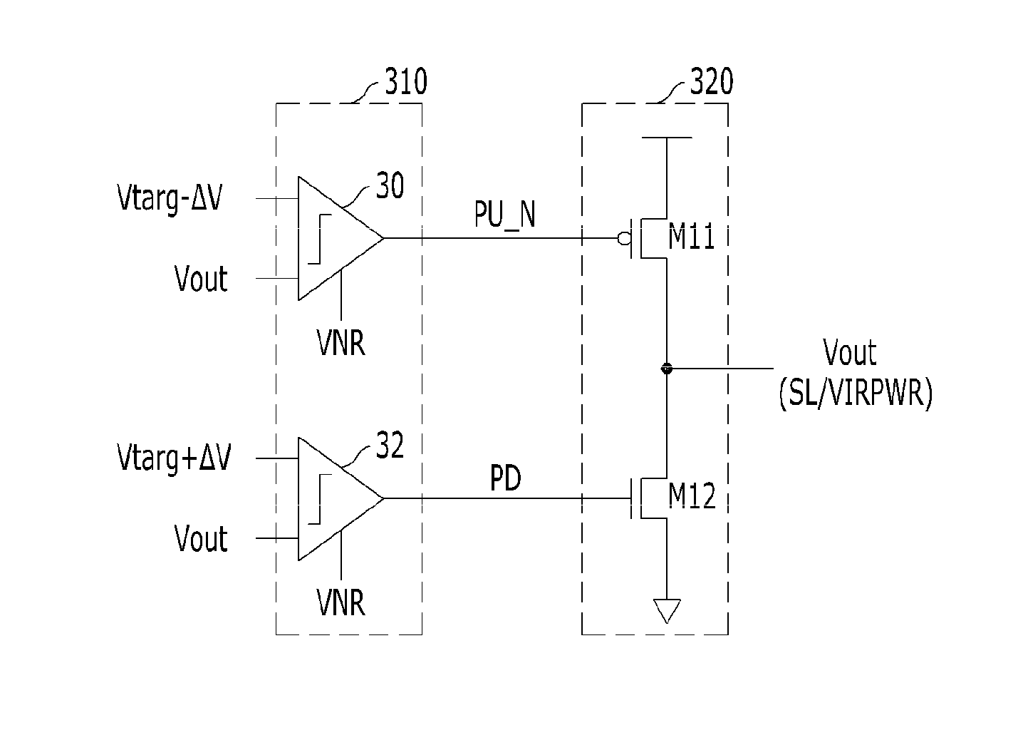
[0029]FIG. 3 is a view showing a core bias line stabilization circuit of a nonvolatile memory device in accordance with an embodiment of the present invention.

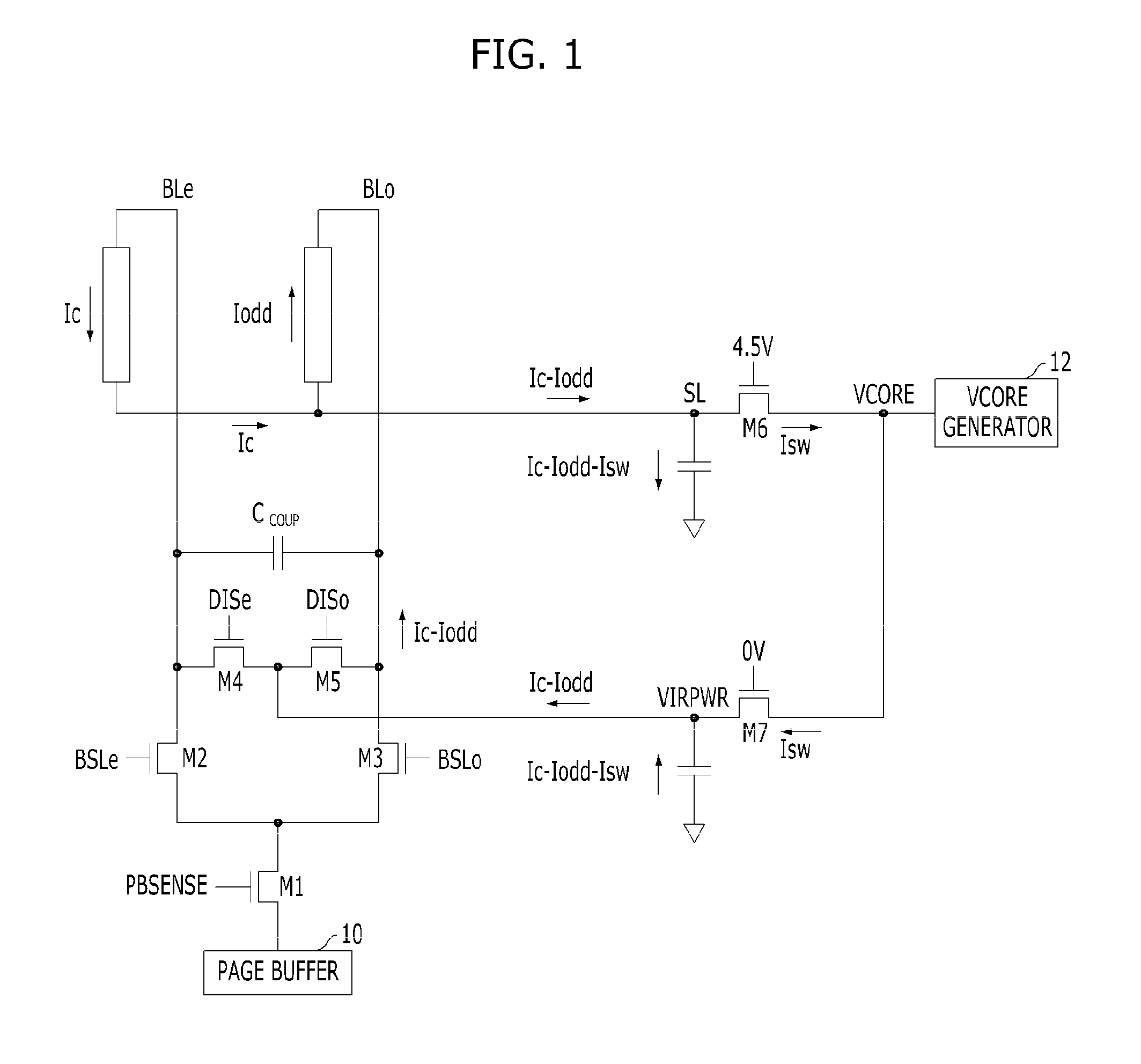
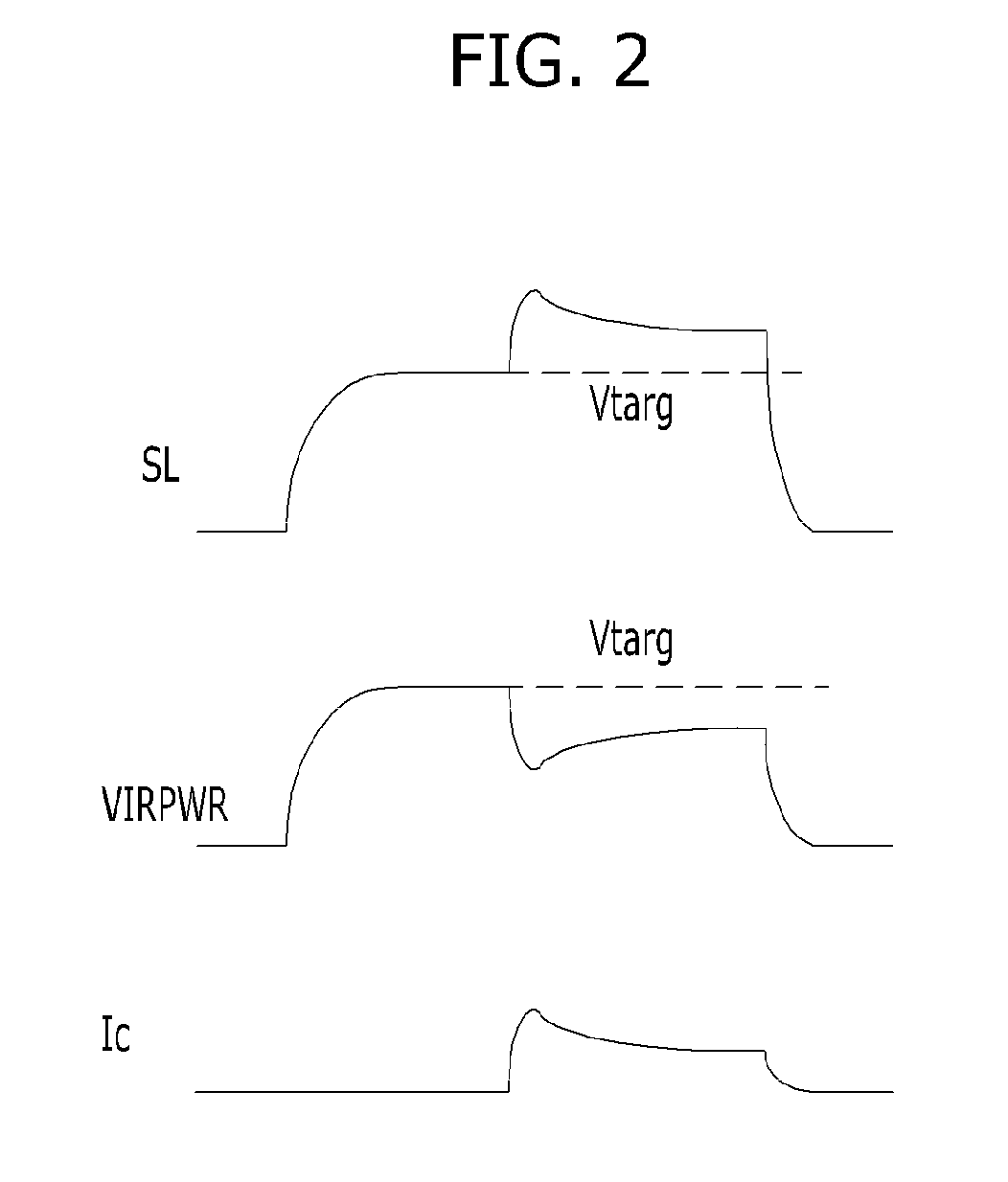
[0030]As shown in FIG. 1, a core voltage generator may be provided. The core voltage generator may generate a core voltage VCORE as a driving voltage of core bias lines SL and VIRPWR. The core bias line stabilization circuit shown in FIG. 3 is added for compensation driving the source line SL or the virtual power line VIRPWR. As such, the cor...


PUM


Abstract

A nonvolatile memory device includes: a driving voltage generation unit configured to generate a driving voltage of a core bias line included in a memory cell current path; a comparison unit configured to compare a voltage level of the core bias line with a predetermined limit level in response to a virtual negative read signal; and a compensation driving unit configured to compensation-drive the core bias line in response to an output signal of the comparison unit.

Description

CROSS-REFERENCE TO RELATED APPLICATIONS[0001]The present application claims priority to Korean Patent Application No. 10-2011-0106599, filed on Oct. 18, 2011, which is incorporated herein by reference in its entirety.BACKGROUND[0002]1. Field of the Invention[0003]Embodiments of the present invention relate to a semiconductor design technology, and more particularly, to a core bias line stabilization circuit of a nonvolatile memory device.[0004]2. Description of the Related Art[0005]A semiconductor integrated circuit (IC) is provided with an internal driving voltage generation block for stably operating various internal logics and devices. In the case of a nonvolatile memory device, in particular, a NAND flash memory, biases with very various levels are needed.[0006]A NAND flash memory performs program and read operations using a distribution of a cell threshold voltage (Vth). Although it is advantageous if the distribution of the cell threshold voltage (Vth) is narrow, as semiconduc...

Claims


Application Information

Patent Timeline
Patent Type & Authority Applications(United States)
IPC IPC(8): G11C7/00
CPCG11C16/30G11C5/147G11C16/06G11C16/26
Inventor AHN, SUNG-HOON
Owner SK HYNIX INC
Features
  • R&D
  • Intellectual Property
  • Life Sciences
  • Materials
  • Tech Scout
  • Unparalleled Data Quality
  • Higher Quality Content
  • 60% Fewer Hallucinations
Learn More