Methods of Forming Organic Light Emitting Structures and Methods of Manufacturing Organic Light Emitting Display Devices

a technology of organic light emitting structure and organic light emitting display device, which is applied in the direction of basic electric elements, semiconductor devices, electrical equipment, etc., can solve the problems of deviation of thickness, leakage current generation, and inability to form organic layers uniformly on the sidewall, so as to reduce crosstalk between adjacent pixel regions, reduce the ability of hole transport or hole injection, and improve the luminescence characteristics

Active Publication Date: 2013-05-02
SAMSUNG DISPLAY CO LTD
View PDF5 Cites 32 Cited by
  • Summary
  • Abstract
  • Description
  • Claims
  • Application Information

AI Technical Summary

Benefits of technology

[0027]According to the exemplary embodiments, a first organic layer including, e.g., a hole injection layer and a hole transport layer may be formed on a whole surface of a lower substrate, and then a PDL may be formed on the first organic layer. An emitting layer may be selectively formed in a pixel region defined by the PDL. Accordingly, a leakage current or deviations of various luminescence characteristics near a sidewall of the PDL may be decreased because the PDL may be formed on the first organic layer. Additionally, an exposure process may be performed selectively on the PDL so that hole transport or hole injection capabilities and an electrical conductivity of a portion of the first organic layer under the PDL may be decreased. Therefore, crosstalk between adjacent pixel regions may be prevented and an OLED device having improved luminescence characteristics, e.g., resolution, contrast, etc., may be obtained.

Problems solved by technology

However, when the organic layers having different materials and characteristics relative to each other make contact with a sidewall of the PDL, the organic layers may not be formed uniformly on the sidewall of the PDL so as to cause, e.g., a deviation of thickness of the organic layers near the sidewall of the PDL.
Accordingly, leakage current may be generated near the sidewall of the PDL and distributions of luminescence characteristics of the OLED device in each pixel region may become irregular.

Method used


Image

  • Methods of Forming Organic Light Emitting Structures and Methods of Manufacturing Organic Light Emitting Display Devices
  • Methods of Forming Organic Light Emitting Structures and Methods of Manufacturing Organic Light Emitting Display Devices
  • Methods of Forming Organic Light Emitting Structures and Methods of Manufacturing Organic Light Emitting Display Devices

Examples


Embodiment Construction

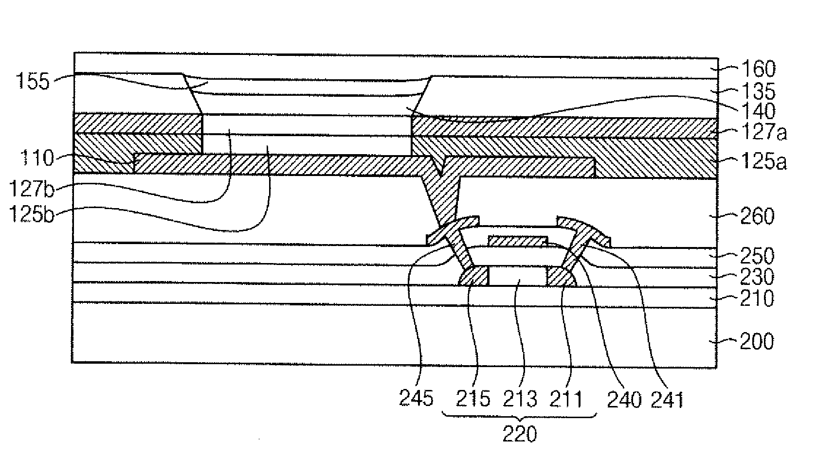
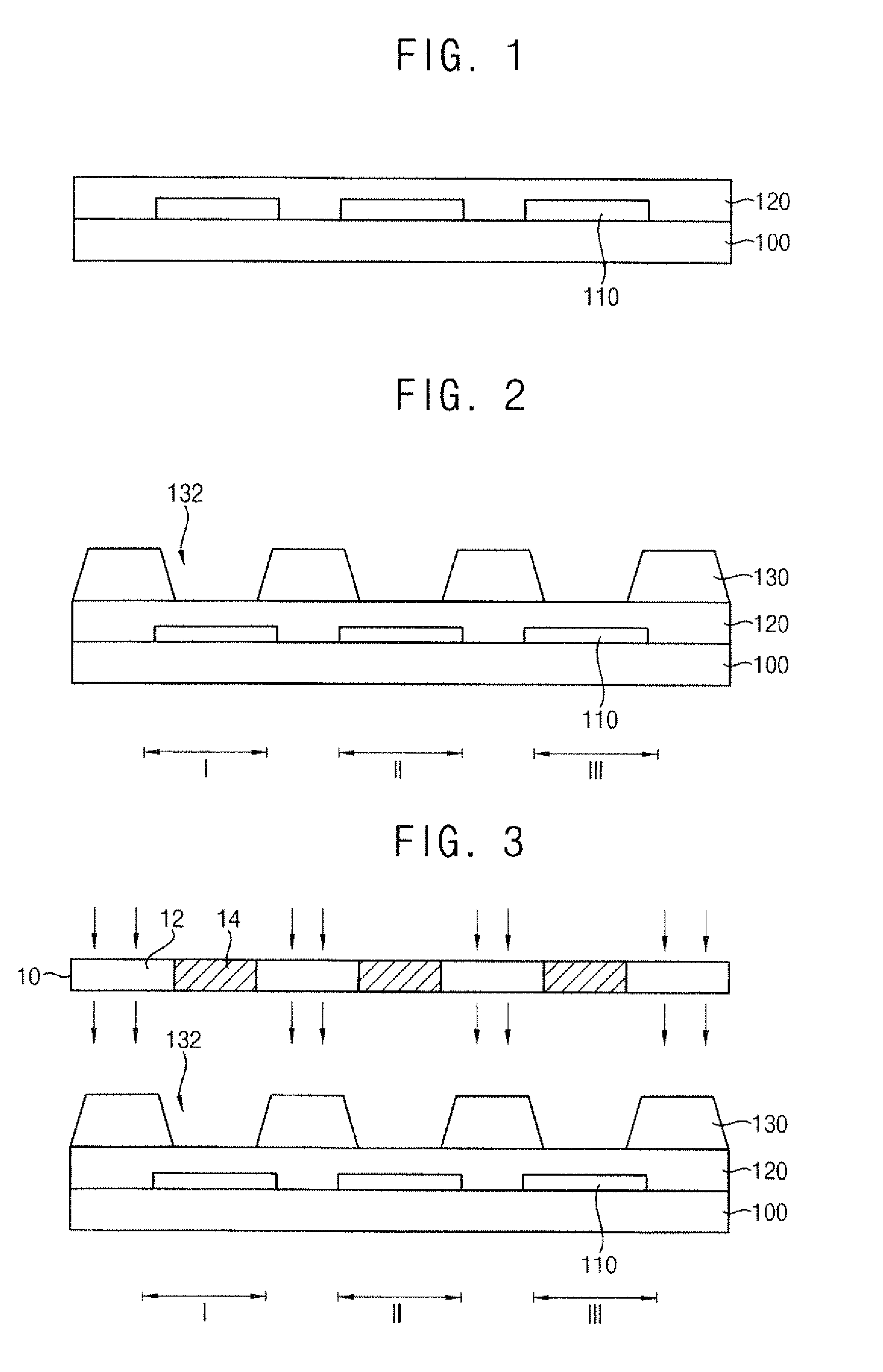
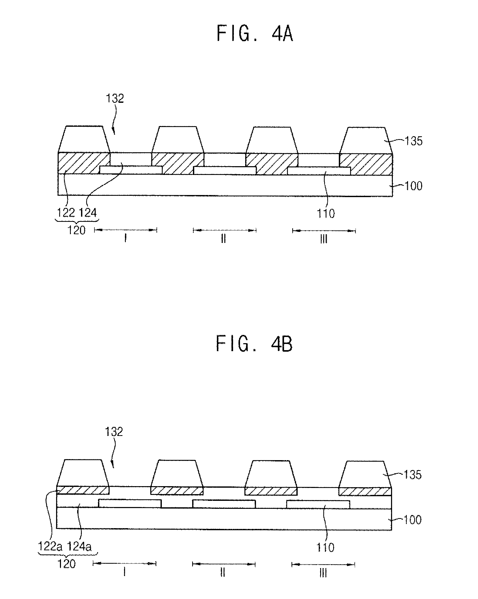
[0031]Various exemplary embodiments will be described more fully hereinafter with reference to the accompanying drawings, in which some exemplary embodiments are shown. The invention may, however, be embodied in many different forms and should not be construed as limited to the exemplary embodiments set forth herein. Rather, these exemplary embodiments are provided so that this description will be thorough and complete, and will fully convey the scope of the invention to those skilled in the art. In the drawings, the sizes and relative sizes of layers and regions may be exaggerated for clarity.

[0032]It will be understood that, when an element or layer is referred to as being “on,”“connected to” or “coupled to” another element or layer, it can be directly on, connected or coupled to the other element or layer, or intervening elements or layers may be present. In contrast, when an element is referred to as being “directly on,”“directly connected to” or “directly coupled to” another el...


PUM


Abstract

In a method of forming an organic light emitting structure, a plurality of first electrodes spaced apart from each other is formed on a lower substrate. A first organic layer covering the first electrodes is formed on the lower substrate. A preliminary pixel defining layer is formed on the first organic layer. The preliminary pixel defining layer includes a photosensitive material, and is selectively exposed to light so that the preliminary pixel defining layer and a portion of the first organic layer beneath the preliminary pixel defining layer are transformed into a pixel defining layer and a first organic layer pattern, respectively. An emitting layer is formed on the first organic layer exposed by the pixel defining layer. A second organic layer is formed on the emitting layer. A second electrode is formed on the second organic layer.

Description

CLAIM OF PRIORITY[0001]This application makes reference to, incorporates the same herein, and claims all benefits accruing under 35 U.S.C. §119 from an application earlier filed in the Korean Intellectual Property Office on the 28 Oct. 2011 and there duly assigned Serial No. 10-2011-0111185.BACKGROUND OF THE INVENTION[0002]1. Field of the Invention[0003]The present invention relates to methods of forming organic light emitting structures and methods of manufacturing organic light emitting display devices. More particularly, the invention relates to organic light emitting structures including a pixel defining layer and organic layers, and methods of manufacturing organic light emitting display devices including a pixel defining layer and organic layers.[0004]2. Description of the Related Art[0005]An organic light emitting display (OLED) device may display desired information such as images, letters and / or characters using a light generated by the combination of holes provided from an...

Claims


Application Information

Patent Timeline
Patent Type & Authority Applications(United States)
IPC IPC(8): H01L51/56
CPCH01L51/5056H01L51/0018H01L27/3246H01L51/5088H10K59/122H10K71/233H10K50/15H10K50/17H10K59/1201
Inventor LEE, DONG-WONSHIN, HYEA-WEON
Owner SAMSUNG DISPLAY CO LTD
Why Eureka
Try Eureka