Device housing package and electronic apparatus employing the same

a technology of electronic equipment and housing package, which is applied in the direction of electrical equipment casing/cabinet/drawer, semiconductor/solid-state device details, semiconductor devices, etc., and can solve problems such as prone to junction

Active Publication Date: 2013-05-23
KYOCERA CORP
View PDF24 Cites 20 Cited by
  • Summary
  • Abstract
  • Description
  • Claims
  • Application Information

AI Technical Summary

Problems solved by technology

In the above-described device housing package, in joining the lid body to the sealing ring by means of seam welding or the like, a stress tends to be concentrated on a junction between the frame body and the sealing ring due to thermal expansion or thermal shrinkage of the frame body, the sealing ring, and the lid body, wherefore the junction is susceptible to a problem such as cracking and separation.

Method used


Image

  • Device housing package and electronic apparatus employing the same
  • Device housing package and electronic apparatus employing the same
  • Device housing package and electronic apparatus employing the same

Examples


modified example 1

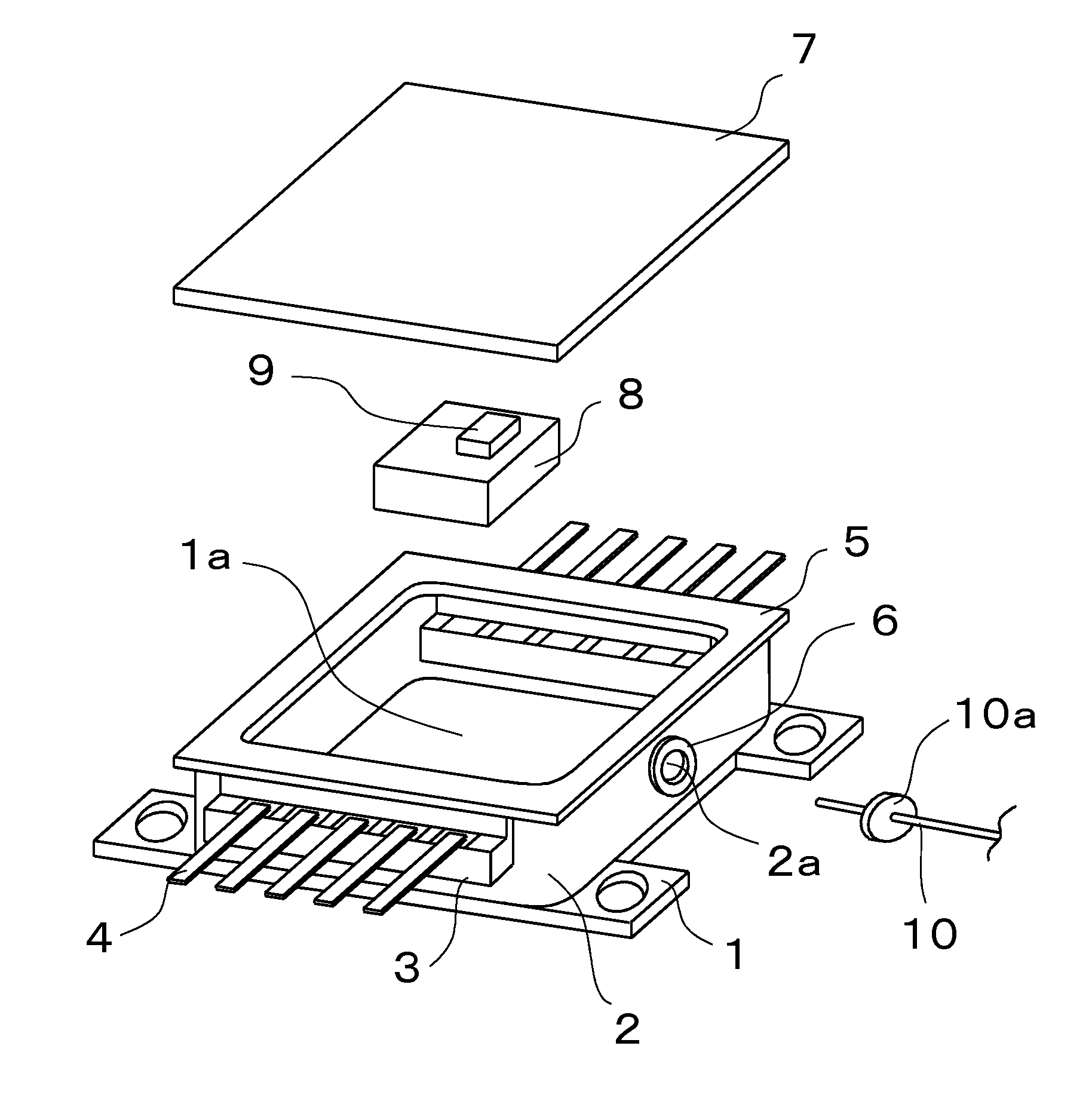
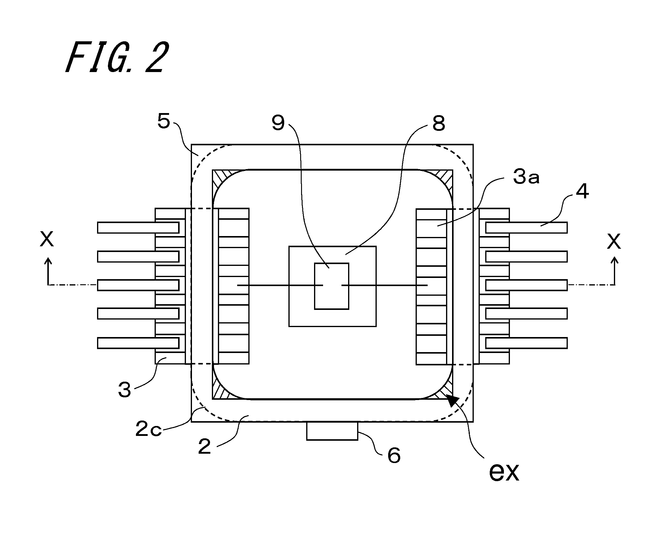
[0075]In the device housing package of Modified example 1 of the embodiment, as shown in FIG. 4, the sealing ring 5 may be made larger in outer shape than the frame body 2 as seen in a plan view so as to extend outward beyond the upper surface of the input-output terminal 3 attached to the notch 2b of the frame body 2. The diagonally shaded area as seen in FIG. 4 represents the exposed part ex of the frame body 2 lying outside the sealing ring 5. Moreover, FIG. 5 is an enlarged view of a main part of the construction, illustrating the condition where the sealing ring 5, which is diagonally shaded, extends outward beyond the upper surface of the input-output terminal 3. Note that the upper surface of the input-output terminal 3 refers to the upper surface of the upstanding wall portion constituting the input-output terminal 3.

[0076]In the case of joining the lid body 5 to the sealing ring 5 by means of seam welding or the like, the heat liberated by the seam welding or the like is no...

modified example 2

[0077]In the device housing package of Modified example 2 of the embodiment, as shown in FIG. 6, the sealing ring 5 may be made larger in outer shape than the frame body 2 as seen in a plan view so as to extend outward beyond the side wall provided with the through hole 2a of the frame body 2. The diagonally shaded area as seen in FIG. 6 represents the exposed part ex of the frame body 2 lying outside the sealing ring 5. Moreover, FIG. 7 is an enlarged view of a main part of the construction, illustrating the condition where the sealing ring 5, which is diagonally shaded, extends outward beyond the side wall provided with the through hole 2a of the frame body 2.

[0078]When the lid body 7 is joined to the sealing ring 5 by means of seam welding or the like, under the heat liberated by the seam welding, thermal expansion or thermal shrinkage takes place due to the difference in thermal expansion coefficient among the frame body 2, the sealing ring 5, and the lid body 7. At this time, d...


PUM


Abstract

A device housing package includes a base body (1) including, at its upper surface, a placement portion (1a) of a semiconductor device (9); a frame body (2) disposed on the base body (1) surrounding the placement portion (1a), including a notch (2b) formed by cutting a side wall thereof; an input-output terminal (3) attached to the notch (2b), including a wiring conductor layer (3a) electrically connected to the semiconductor device (9); and a sealing ring (5) disposed on an upper portion of the frame body (2). Moreover, side walls of the frame body (2) have, when seen in a plan view, an outer corner (2c) of adjacent side walls having a curved surface, the outer corner (2c) lying within a region overlapping the sealing ring (5) as seen in a plan view.

Description

TECHNICAL FIELD[0001]The present invention relates to a device housing package for use in, for example, a device housing package for containing a semiconductor device, and an electronic apparatus which employs the device housing package.BACKGROUND ART[0002]Some device housing packages are of a type constructed by bonding a lid body to the upper surface of a frame body through a sealing ring. Such a device housing package is disclosed in, for example, Japanese Unexamined Patent Publication JP-A 11-145317 (1999).[0003]In the above-described device housing package, in joining the lid body to the sealing ring by means of seam welding or the like, a stress tends to be concentrated on a junction between the frame body and the sealing ring due to thermal expansion or thermal shrinkage of the frame body, the sealing ring, and the lid body, wherefore the junction is susceptible to a problem such as cracking and separation.[0004]An object of the invention is to provide a device housing packag...

Claims


Application Information

Patent Timeline
Patent Type & Authority Applications(United States)
IPC IPC(8): H05K5/00H05K7/02
CPCH01L23/057H01L23/10H05K5/0091H05K7/02H01L2224/48091H01L2924/00014H01L2224/48245
Inventor SATAKE, TAKEO
Owner KYOCERA CORP
Why Eureka
Try Eureka