Color filter array on pixel array substrate and display panel

a color filter array and substrate technology, applied in the field of color filter arrays on pixel array substrates and display panels, can solve the problems of limiting the overall color adjustment flexibility of the lcd, and the inability to optimize the display color of the lcd, so as to achieve favorable color performance, improve the chromaticity of the color filter array, and increase the transmission of light through the color filter patterns

Inactive Publication Date: 2013-05-23
AU OPTRONICS CORP
View PDF10 Cites 28 Cited by
  • Summary
  • Abstract
  • Description
  • Claims
  • Application Information

AI Technical Summary

Benefits of technology

[0011]Based on the above, the wavelength converting layer is configured in the color filter array on pixel array substrate and in the display panel according to the invention. The wavelength converting layer is disposed corresponding to the color filter patterns and converts the spectrum of light before the light passes through the color filter patterns. Thereby, the transmittance of light passing through the color filter patterns can be increased. As a result, the chromaticity of the color filter array can be improved, and thereby the display panel can display images with favorable color performance.

Problems solved by technology

Nonetheless, the transmittance of light varies when the light passes through each color resist of the color filter, and the varied transmittances cannot be easily increased, thus limiting the overall color adjustment flexibility of the LCD.
As a result, the display color of the LCD cannot be optimized.

Method used


Image

  • Color filter array on pixel array substrate and display panel
  • Color filter array on pixel array substrate and display panel
  • Color filter array on pixel array substrate and display panel

Examples


experimental examples

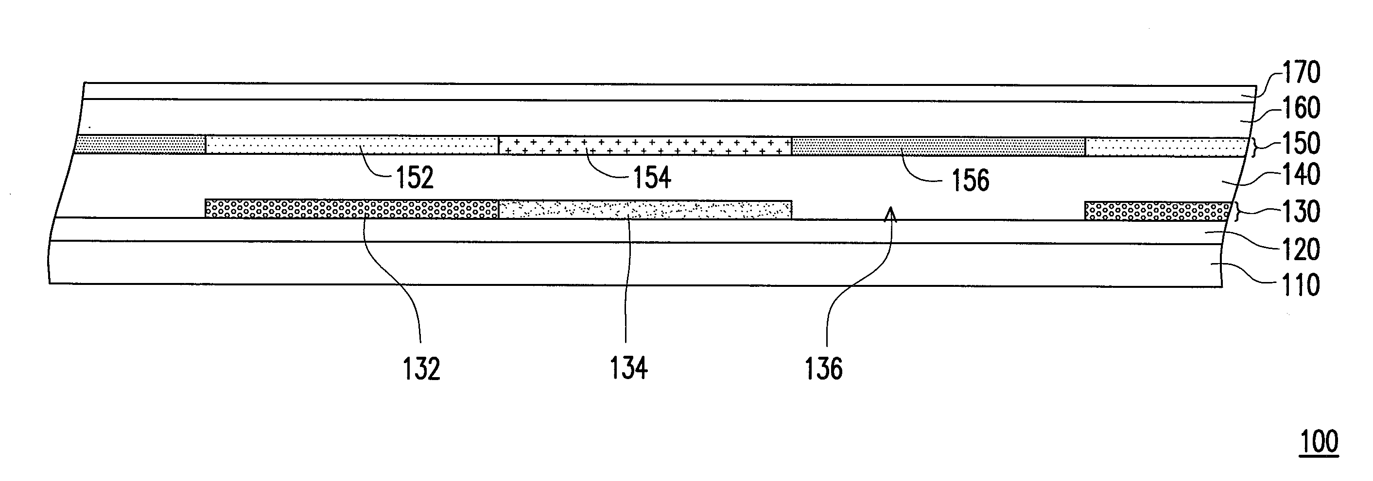
[0029]To verify that the display panel described in the previous embodiments of the invention is capable of improving the transmittance of light (provided by the backlight module) passing through the red and green color filter patterns, experimental examples 1, 2, and a comparison example are provided herein for comparison. In the experimental examples 1 and 2, the display panel has the structure as shown in FIG. 2. The first wavelength converting patterns are made of DCM, and the second wavelength converting patterns are made of fluorescent coumarin 30. The first color filter patterns are red filter patterns, and the second color filter patterns are green filter patterns. The amount of the wavelength converting material in the first and second wavelength converting patterns accounts for 5% in the experimental example 1, while the amount of the wavelength converting material in the first and second wavelength converting patterns accounts for 50% in the experimental example 2. The st...


PUM


Abstract

A color filter array on pixel array substrate includes a substrate, an active device array, a wavelength converting layer, a first passivation layer, a second passivation layer, a color filter array, and a pixel electrode layer. The active device array is disposed on the substrate. The wavelength converting layer is disposed on the active device array and includes at least one first wavelength converting pattern. The first passivation layer is disposed on the wavelength converting layer and the active device array and covers the first wavelength converting pattern and the active device array. The color filter array is disposed on the first passivation layer and includes a plurality of first, second, and third color filter patterns disposed alternately. The first wavelength converting pattern is disposed corresponding to one first color filter pattern. The second passivation layer and the pixel electrode layer are sequentially disposed on the color filter array.

Description

CROSS-REFERENCE TO RELATED APPLICATION[0001]This application claims the priority benefit of Taiwan application serial no. 100142013, filed on Nov. 17, 2011. The entirety of the above-mentioned patent application is hereby incorporated by reference herein and made a part of this specification.BACKGROUND OF THE INVENTION[0002]1. Field of the Invention[0003]The invention is related to a pixel array substrate and a display panel, and in particular to a color filter array on pixel array substrate and a display panel.[0004]2. Description of Related Art[0005]With advantages of high definition, small volume, light weight, low driving voltage, low power consumption, and a wide range of applications, a liquid crystal display (LCD) has replaced a cathode ray tube (CRT) display and has become the mainstream display product in the next generation. The LCD is mainly composed of an LCD panel and a backlight module. The planar light source (e.g., a white light source in most cases) provided by the ...

Claims


Application Information

Patent Timeline
Patent Type & Authority Applications(United States)
IPC IPC(8): G09F13/04G02B5/22
CPCG02F1/133514G02F2202/046G02F2001/133614G02F1/133617G02F1/133614
Inventor LIN, SHIUAN-FU
Owner AU OPTRONICS CORP
Why Eureka
Try Eureka