Method for manufacturing quantum dots display panel

a display panel and quantum dots technology, applied in the field of display technology, can solve the problems of not being able to be mass-produced, and achieve the effects of large-scale volume production, high-resolution graphics, and simple making process

Active Publication Date: 2018-02-01
TCL CHINA STAR OPTOELECTRONICS TECH CO LTD
View PDF1 Cites 14 Cited by
  • Summary
  • Abstract
  • Description
  • Claims
  • Application Information

AI Technical Summary

Benefits of technology

[0006]The present disclosure provide a method for manufacturing a quantum dots display panel, preparation of raw materials and simple in making process, high-resolution graphics, large-scale volume production, and processing time and cost are saved.
[0038]The present disclosure has the following advantages: the present disclosure provide a method for manufacturing quantum dots display panel, using an existing yellow light manufacturing process from color filter or combining with a dry etching manufacturing process to resin composition with surface-modified red quantum dots and surface-modified green quantum dots, then completing production of a quantum dots layer with a more refined graphical structure. Compared with other existing method for manufacturing quantum dots display panel, the present disclosure has the following advantages that preparation of raw materials and simple in making process, high-resolution graphics, large-scale volume production, and processing time and cost are saved, and introducing quantum dots into structure of color filter is effectively improve color saturation and gamut of display device, enhance color performance of display panel.

Problems solved by technology

In addition to the above-described method, produced quantum dots pattern also can by transfer or screen printing, however resolution of quantum dots pattern by transfer is low, the edge is jagged, and adhesion between quantum dots layer and substrate remains to be improved; the ink-jet printing method for quantum dots layer pattern is demanding the equipment, how to ensure stability of Ink-jet ink droplet and printing accuracy still has technical barriers and they can't be mass-produced.

Method used


Image

  • Method for manufacturing quantum dots display panel
  • Method for manufacturing quantum dots display panel
  • Method for manufacturing quantum dots display panel

Examples


first embodiment

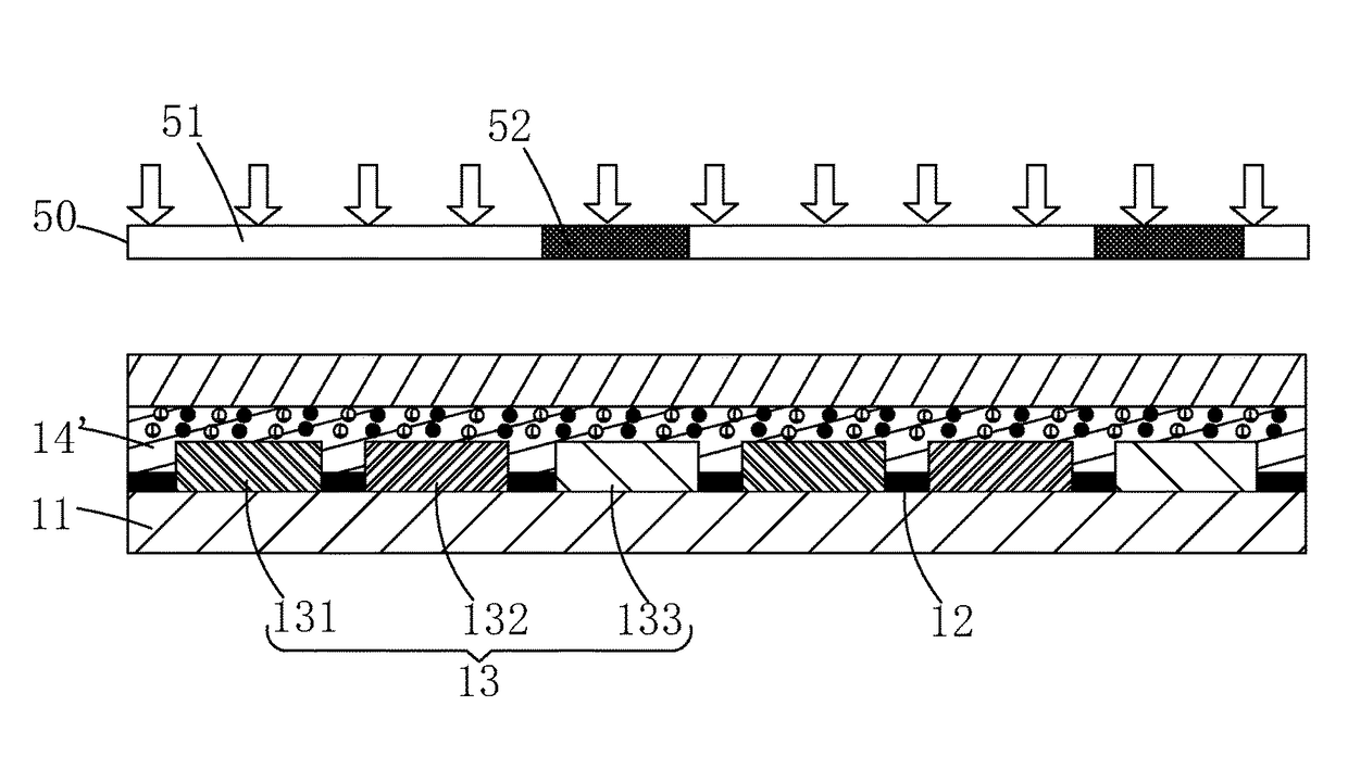
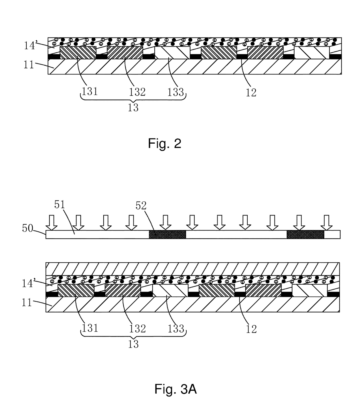
[0060]Specifically, shown in FIG. 5, in the quantum dots display panel of the step 4 the backlight used in the display device is blue. Backlight module 2 emits blue backlight. While the blue backlight is exciting, the quantum dots layer 14 mixing with the red and green quantum dots is emitting the red and green mixed light with the narrow FWHM. The mixed light is then passed through the red colored barrier layer 131, the green colored barrier layer 132, then is filtered into the high-purity red monochromatic light and the green monochromatic light to display red and green. The transparent light resistance layer 133, which is not covered by the quantum dots layer, displays blue directly from the blue backlight. Finally the desired red, green, and blue color by the color display is provided, and the display color gamut index is effectively improved. The quantum dots layer 14 does not include blue quantum dots material, but it uses the blue backlight matched with the transparent light ...

second embodiment

[0065]In the method for manufacturing quantum dots display panel according to the present disclosure, the step 3 of combining the yellow light manufacturing process with the dry etching manufacturing process to perform patterning processing on the quantum dots film 14′, the step 3 specifically including the steps of:

[0066]Step 31′, after pre-baking in step 2, baking the color film substrate at a temperature of 200-250 DEG C. to fully cure the quantum dots film 14′;

[0067]Step 32′, using a spin coating method or a slit coating method to coat a layer of transparent photoresist material (such as W photoresist, PFA photoresist) uniformly on the quantum dots film 14′ after pre-baking; providing a light mask 50, and using the light mask 50 to perform development process and exposure process of the transparent photoresist material to obtain a patterned photoresist layer 15; wherein the light mask 50 includes a transmitting portion 51 corresponding to the red colored barrier layer 131 and th...


PUM

PropertyMeasurementUnit
temperatureaaaaaaaaaa

Abstract

A method for manufacturing quantum dots display panel comprises the following steps of: using an existing yellow light manufacturing process from color filter or combining with a dry etching manufacturing process to resin composition with surface-modified red quantum dots and surface-modified green quantum dots, then completing production of a quantum dots layer with a more refined graphical structure. Compared with other existing method for manufacturing quantum dots display panel, the present disclosure has the following advantages that simple preparation of raw materials and in making process, high-resolution graphics, large-scale volume production, and less processing time and cost are saved. The quantum dots are used into the structure of the color filter is to effectively improve color saturation and gamut of the display device, and to enhance color performance of display panel.

Description

FIELD OF THE DISCLOSURE[0001]The present disclosure relates to a display technology field, and more particularly to a method for manufacturing quantum dots display panel.BACKGROUND OF THE DISCLOSURE[0002]With the continuous development of display technology, and people require the quality of display increasing, the quantum dots (QDs), also known, is a kind of spherical or spherical semiconductor nanocrystals composed by group II-VI or group III-V, usually between several nanometers to several tens of nanometers due QDs particle size of less than or close to the exciton Bohr radius corresponding material, resulting in a quantum confinement effect its energy level structure from a quasi-continuous material into discrete quantum dots material structure, resulting QDs exhibit special stimulated luminescent properties. As the size of the QDs is reduced, increasing the band gap energy level, the corresponding excited QDs and quantum energy required points excited to the ground state energ...

Claims


Application Information

Patent Timeline
Patent Type & Authority Applications(United States)
IPC IPC(8): G02F1/1335G02F1/1339B05D1/00G02F1/1368
CPCG02F1/133516G02F1/1368G02F1/133514G02F1/133512G02F1/133528G02F1/1339G02F1/133617B05D1/005G02F2202/36G02F2202/10G02F2001/133531G02F2001/133614G02F1/133621G02F1/133531G02F1/1362G09G3/00G02F1/1335G02F1/133614
Inventor LIU, GUOHE
Owner TCL CHINA STAR OPTOELECTRONICS TECH CO LTD
Why Eureka
Try Eureka