Method for producing semiconductor device

a technology of semiconductor wafers and under-fill sheets, which is applied in the direction of semiconductor devices, electrical equipment, basic electric elements, etc., can solve the problems of reducing the degree of adhesion of the under-fill sheet to the semiconductor wafer, reducing the connection reliability between the semiconductor element and the adherend, and generating voids (air bubbles). , to achieve the effect of high connection reliability, efficient production and facilitation of penetration of the connection member into the under-fill material

Inactive Publication Date: 2013-06-20
NITTO DENKO CORP
View PDF10 Cites 17 Cited by
  • Summary
  • Abstract
  • Description
  • Claims
  • Application Information

AI Technical Summary

Benefits of technology

[0009]First, in the process described above, a circuit surface of a semiconductor wafer and an under-fill sheet are bonded together, and therefore the under-fill sheet is required to closely contact the surface of the semiconductor wafer by following raised and recessed portions thereof. However, as the number of spacing structures such as a bump on the semiconductor wafer increases and circuits become smaller, the degree of adhesion of the under-fill sheet to the semiconductor wafer decreases, so that voids (air bubbles) are generated in between the semiconductor wafer and the under-fill sheet in some cases. If air bubbles are present at an interface between the semiconductor wafer and the under-fill material, air bubbles may expand when a decompressing treatment or a heating treatment is carried out in subsequent steps, thereby reducing adhesion between the semiconductor wafer and the under-fill material, and resultantly the connection reliability between the semiconductor element and the adherend may be decreased when the semiconductor element is mounted on the adherend. If moisture at the time of back surface grinding or dicing of the semiconductor wafer are immixed into air bubbles, the moisture may be vaporized to grow or expand air bubbles when a heating step is subsequently carried out, thereby again decreasing the connection reliability between the semiconductor element and the adherend.
[0044]In the production method, the viscosity of the under-fill material at 23° C. before heat curing is preferably 0.01 MPa·s or more and 100 MPa·s or less. The under-fill material before heat curing has such a viscosity, whereby the retention property of a semiconductor wafer at the time of dicing and the handling property at the time of operation can be improved.

Problems solved by technology

However, as the number of spacing structures such as a bump on the semiconductor wafer increases and circuits become smaller, the degree of adhesion of the under-fill sheet to the semiconductor wafer decreases, so that voids (air bubbles) are generated in between the semiconductor wafer and the under-fill sheet in some cases.
If air bubbles are present at an interface between the semiconductor wafer and the under-fill material, air bubbles may expand when a decompressing treatment or a heating treatment is carried out in subsequent steps, thereby reducing adhesion between the semiconductor wafer and the under-fill material, and resultantly the connection reliability between the semiconductor element and the adherend may be decreased when the semiconductor element is mounted on the adherend.
If moisture at the time of back surface grinding or dicing of the semiconductor wafer are immixed into air bubbles, the moisture may be vaporized to grow or expand air bubbles when a heating step is subsequently carried out, thereby again decreasing the connection reliability between the semiconductor element and the adherend.

Method used


Image

  • Method for producing semiconductor device
  • Method for producing semiconductor device
  • Method for producing semiconductor device

Examples


first embodiment

Providing Step

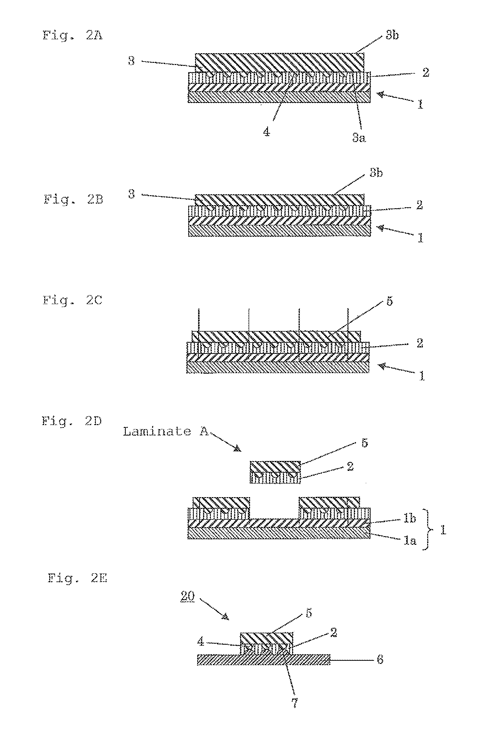
[0051]In a providing step, a sealing sheet including a support and an under-fill material laminated on the support is provided. As the support, a base material, a back surface grinding tape, a dicing tape or the like can be suitably used. This embodiment will be described taking as an example a case where a back surface grinding tape is used.

(Sealing Sheet)

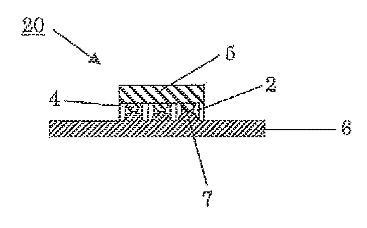
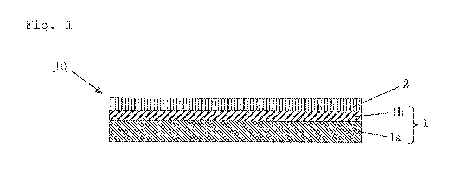
[0052]As shown in FIG. 1, a sealing sheet 10 includes aback surface grinding tape 1 and an under-fill material 2 laminated on the back surface grinding tape 1. The under-fill material 2 is not necessarily laminated on the entire surface of the back surface grinding tape 1 as shown in FIG. 1, but may be provided in a size sufficient for bonding with a semiconductor wafer 3 (see FIG. 2A).

(Back Surface Grinding Tape)

[0053]The back surface grinding tape 1 includes a base material 1a and a pressure-sensitive adhesive layer 1b laminated on the base material 1a. The under-fill material 2 is laminated on the pressure-sensiti...

second embodiment

[0129]In this embodiment, a bonding step of bonding together a circuit surface 3a of a semiconductor wafer 3, on which a connection member 4 is formed, and an under-fill material 2 of the sealing sheet 10 under a reduced pressure of 1000 Pa or less (see FIG. 2A) may be employed in place of the heat pressure-bonding step in the first embodiment. Except for this modification, a predetermined semiconductor device can be produced through the same steps as in the first embodiment, but other preferred aspects will be described.

[0130]The method for bonding is not particularly limited, but a method by pressure-bonding is preferable. Pressure-bonding is carried out normally by pressing the semiconductor wafer and the sealing sheet under a load of pressure of preferably 0.1 to 1 MPa, more preferably 0.2 to 0.7 MPa, by known pressing means such as a pressure-bonding roll. At this time, pressure-bonding may be performed while heating to about 40 to 100° C.

[0131]In this embodiment, the semicondu...

third embodiment

[0135]In the first embodiment, aback surface grinding tape is used as a support, whereas in this embodiment, a dicing tape including a base material and a pressure-sensitive adhesive layer laminated on the base material is used as a support. In this case, a predetermined semiconductor device can be produced through the same steps as in the first embodiment and the second embodiment except that a semiconductor wafer having an intended thickness is used to omit the grinding step (i.e. steps in FIGS. 2B to 2E excluding the step in FIG. 2A).


PUM


Abstract

There is provided a method for producing a semiconductor device, capable of suppressing generation of voids at an interface between a semiconductor element and an under-fill sheet to produce a semiconductor device with high reliability. The method includes providing a sealing sheet having a support and an under-fill material laminated on the support; thermally pressure-bonding a circuit surface of a semiconductor wafer, on which a connection member is formed, and the under-fill material of the sealing sheet under conditions of a reduced-pressure atmosphere of 10000 Pa or less, a bonding pressure of 0.2 MPa or more and a heat pressure-bonding temperature of 40° C. or higher; dicing the semiconductor wafer to form a semiconductor element with the under-fill material; and electrically connecting the semiconductor element and the adherend through the connection member while filling a space between the adherend and the semiconductor element using the under-fill material.

Description

BACKGROUND OF THE INVENTION[0001]1. Field of the Invention[0002]The present invention relates to a method for producing a semiconductor device.[0003]2. Description of the Related Art[0004]In recent years, demands for high-density mounting have been increased as electronic instruments have become smaller and thinner. For meeting the demands, a method is employed in which a back surface (surface opposite to a circuit surface on which a pattern is formed) of a semiconductor wafer is ground to make a semiconductor device thinner. Back surface grinding of the semiconductor wafer is carried out generally by bonding a back surface grinding tape to the circuit surface of the semiconductor wafer and subjecting the back surface of the semiconductor wafer to grind processing.[0005]On the other hand, for semiconductor packages, the surface mount method has become mainstream suitable for high-density mounting in place of the conventional pin insertion method. In the surface mount method, a lead ...

Claims


Application Information

Patent Timeline
Patent Type & Authority Applications(United States)
IPC IPC(8): H01L21/78
CPCH01L2224/27848H01L2221/68381H01L2224/29371H01L2224/29324H01L2224/2783H01L24/13H01L24/16H01L24/27H01L24/29H01L24/32H01L21/6836H01L24/73H01L24/81H01L24/83H01L24/94H01L2224/13111H01L2224/13144H01L2224/13147H01L2224/2929H01L2224/29311H01L2224/29316H01L2224/29339H01L2224/29344H01L2224/29347H01L2224/29355H01L2224/29364H01L2224/29387H01L2224/29388H01L2224/29393H01L2224/32225H01L2224/32245H01L2224/81203H01L2224/83191H01L2224/83862H01L2224/94H01L2224/29318H01L2221/68377H01L2221/6834H01L2221/68336H01L2221/68327H01L2224/27003H01L2924/3641H01L2224/73104H01L2224/16245H01L2224/16225H01L21/563H01L21/78H01L2224/11H01L2224/27H01L2924/01082H01L2924/01047H01L2924/01029H01L2924/0103H01L2924/01083H01L2924/15787H01L2924/00H01L21/30
Inventor MORITA, KOSUKETAKAMOTO, NAOHIDESENZAI, HIROYUKI
Owner NITTO DENKO CORP
Why Eureka
Try Eureka