Semiconductor device and method of manufacturing the same

Active Publication Date: 2013-06-27
SK HYNIX INC
View PDF9 Cites 41 Cited by
  • Summary
  • Abstract
  • Description
  • Claims
  • Application Information

AI Technical Summary

Benefits of technology

[0005]The present invention is directed to a three-dimensional (3D) semiconduc

Problems solved by technology

However, there are physical limitations to reducing the size of the memory cells.
However,

Method used


Image

  • Semiconductor device and method of manufacturing the same
  • Semiconductor device and method of manufacturing the same
  • Semiconductor device and method of manufacturing the same

Examples


Example

[0016]The present invention will be described more fully hereinafter with reference to the accompanying drawings, in which exemplary embodiments of the invention are shown. This invention may, however, be embodied in different forms and should not be construed as limited to the embodiments set forth herein. Rather, these embodiments are provided so that this disclosure will be thorough and complete and will fully convey the concept of the invention to those of ordinary skill in the art. The scope of the invention is defined in the claims and their equivalents.

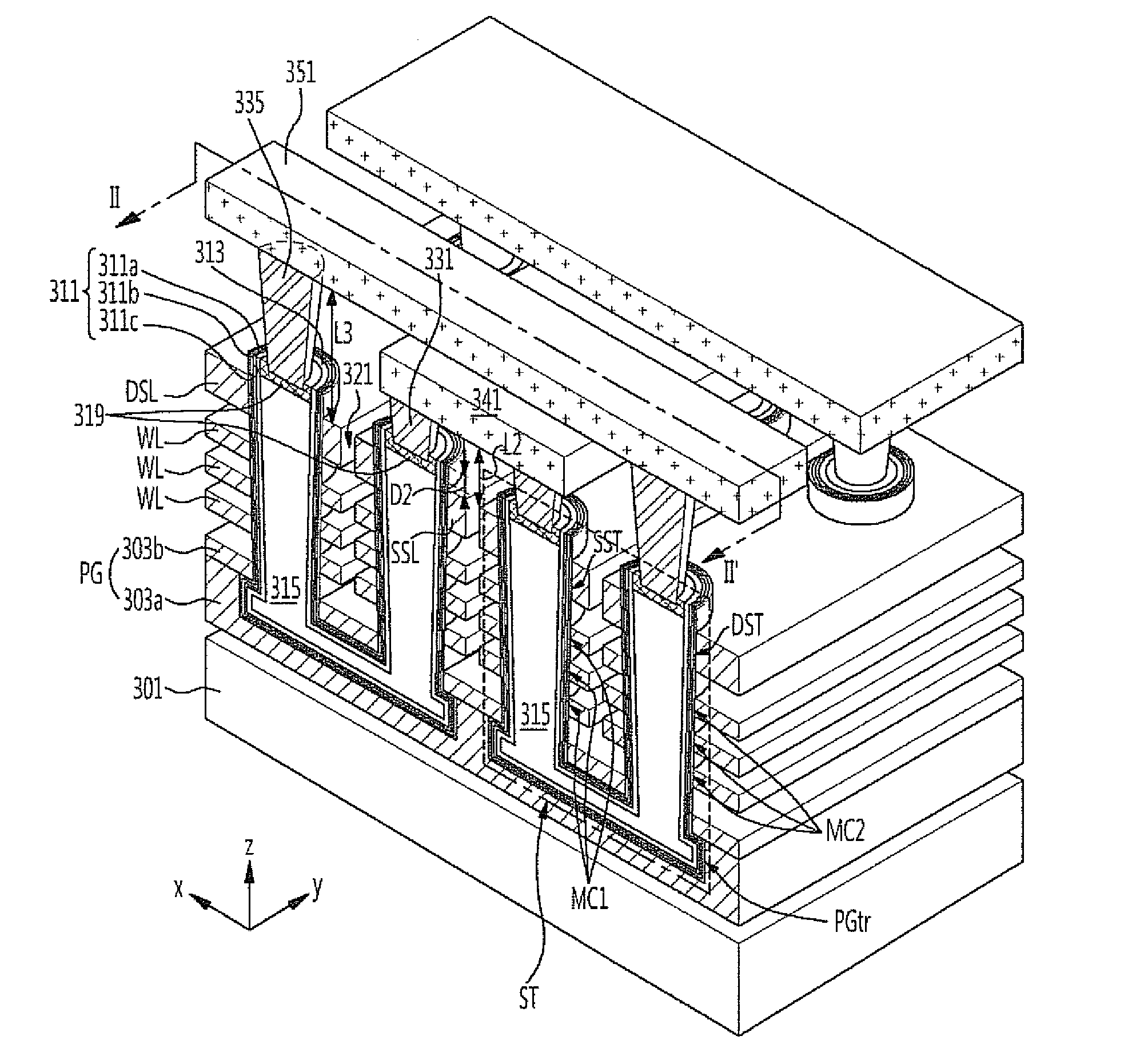
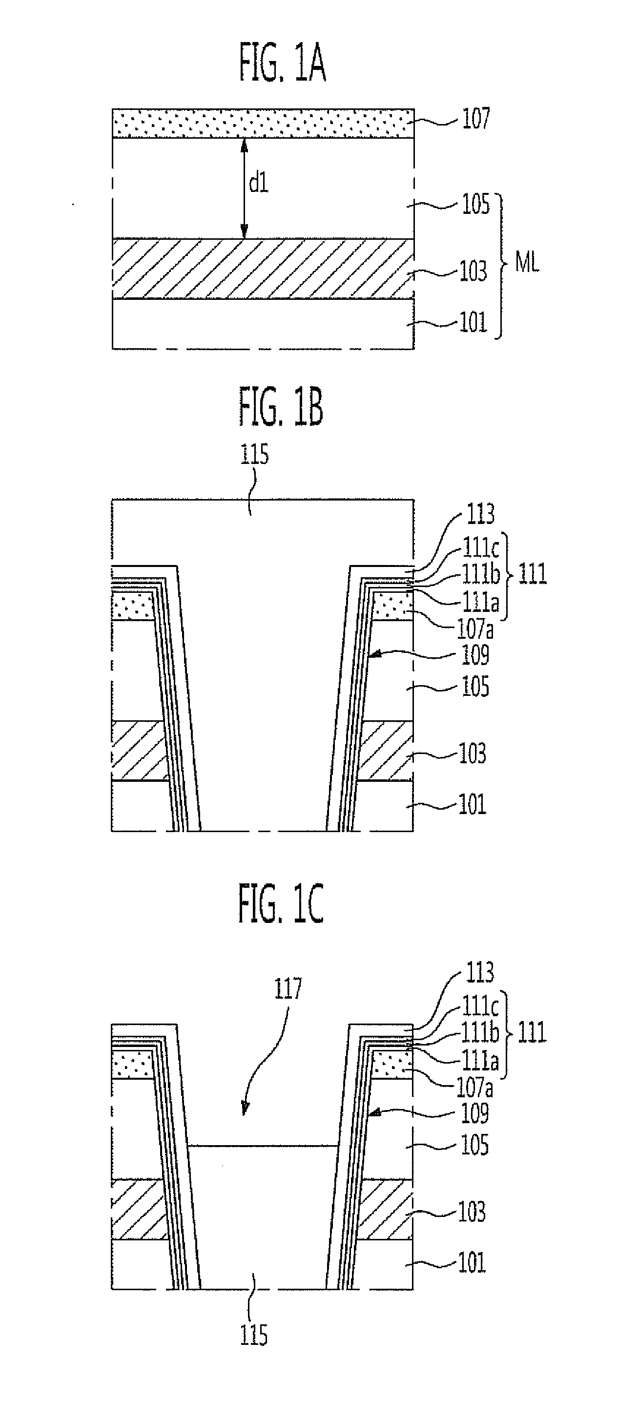
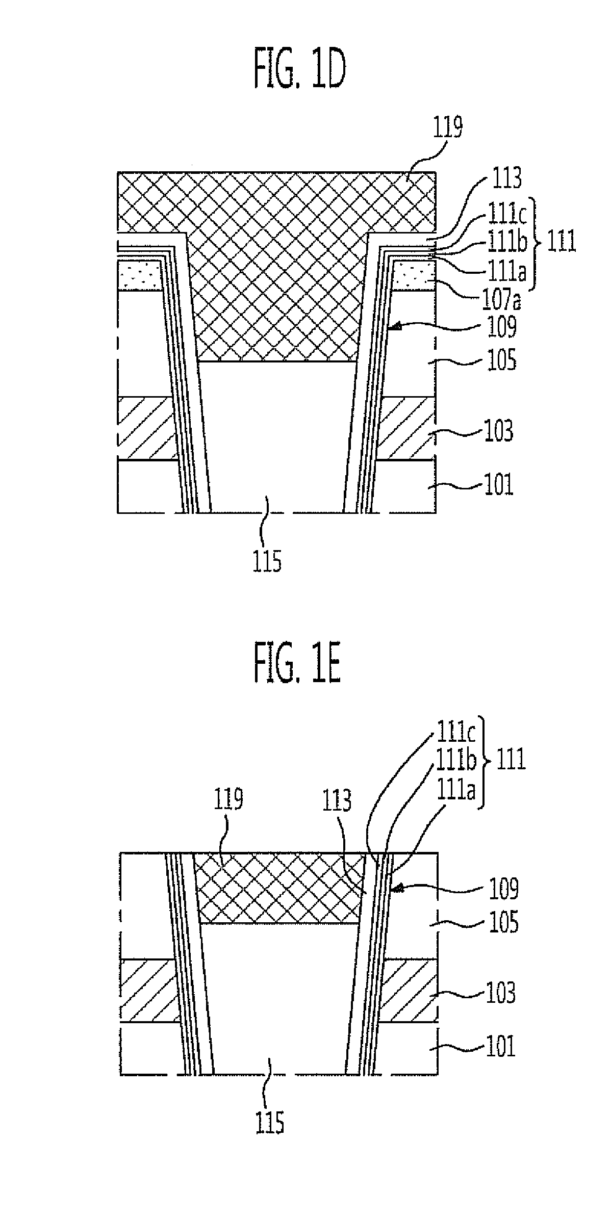
[0017]FIGS. 1A to 1F are cross-sectional views illustrating a method of manufacturing a semiconductor device according to an exemplary embodiment of the present invention. In particular, FIGS. 1A to 1F are cross-sectional views illustrating a method of forming a select transistor area of a semiconductor device according to an exemplary embodiment of the present invention.

[0018]Referring to FIG. 1A, a multilayered structure ML i...


PUM


Abstract

A three-dimensional (3D) semiconductor device includes first interlayer dielectric layers and word lines that are alternately stacked on a substrate; select lines formed on the first interlayer dielectric layers and the word lines; etch stop patterns formed on the select lines to contact the select lines; channel holes formed to pass through the select lines, the first interlayer dielectric layers, and the word lines; channel layers formed on surfaces of the channel holes; insulating layers formed in the channel holes, the insulating layers having an upper surface that is lower than upper surfaces of the etch stop patterns; impurity-doped layers formed in channel holes on upper surface of the insulating layers; and a second interlayer dielectric layer formed over the etch stop patterns and the impurity-doped layers.

Description

CROSS-REFERENCE TO RELATED APPLICATION[0001]This application claims priority to and the benefit of Korean Patent Application No. 10-2011-0139981, filed on Dec. 22, 2011, the disclosure of which is incorporated herein by reference in its entirety.BACKGROUND[0002]The present invention relates to a semiconductor device and a method of manufacturing the same. More specifically, the present invention relates to a three-dimensional (3D) semiconductor device and a method of manufacturing the same.Discussion of Related Art[0003]As there is a growing need to increase the integration degrees of semiconductor devices, various techniques have been developed to increase the integration degrees of semiconductor devices. As a representative method, the integration degree of memory cells is increased within a limited space by reducing the sizes of the memory cells that are two-dimensionally disposed on a semiconductor substrate. However, there are physical limitations to reducing the size of the me...

Claims


Application Information

Patent Timeline
IPC IPC(8): H01L21/336H01L29/78
CPCH01L29/78H01L29/7926H01L29/66833H01L27/1158H10B43/23H10B43/27H01L21/76205
Inventor BIN, JIN HOLEE, KI HONG
Owner SK HYNIX INC
Why Eureka
Try Eureka