Nonvolatile memory device and method of manufacturing the same

a memory device and non-volatile technology, applied in the field of semiconductor devices, can solve the problems of limited time taken for the exposure process, limited memory cell size reduction,

Active Publication Date: 2013-06-27
SK HYNIX INC
View PDF4 Cites 115 Cited by
  • Summary
  • Abstract
  • Description
  • Claims
  • Application Information

AI Technical Summary

Problems solved by technology

But, a reduction in the size of the memory cells arranged in a 2-D way is limited.
If the thickness of the photoresist layer increases, there is a problem in that the time taken for the exposure process is increased.
Furthermore, there are problems in that the

Method used


Image

  • Nonvolatile memory device and method of manufacturing the same
  • Nonvolatile memory device and method of manufacturing the same
  • Nonvolatile memory device and method of manufacturing the same

Examples


Embodiment Construction

[0025]Hereinafter, exemplary embodiments of the present disclosure will be described in detail with reference to the accompanying drawings. The figures are provided to allow those having ordinary skill in the art to understand the scope of the embodiments of the disclosure.

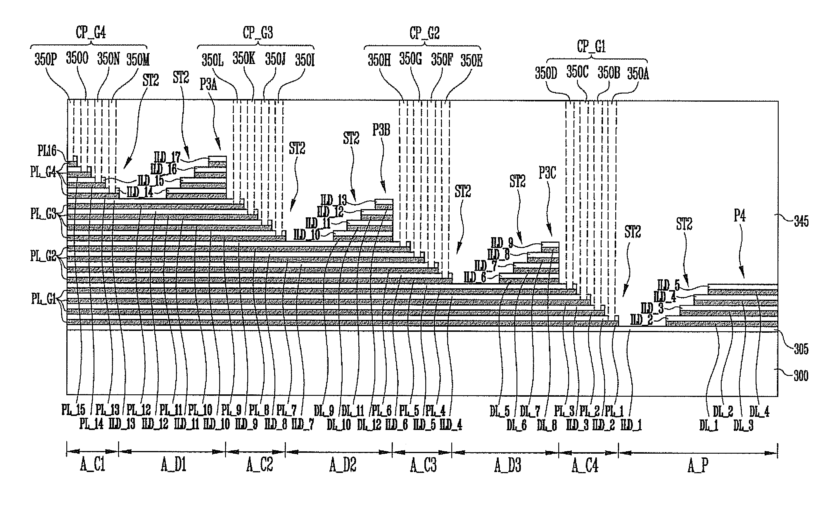
[0026]FIG. 2 is a perspective view illustrating a 3-D nonvolatile memory device according to one embodiment of the present invention. In FIG. 2, only contact regions and part of a cell region coupled to the contact regions and part of a peripheral region are illustrated, and some of insulating layers are not shown, for convenience of description.

[0027]Referring to FIG. 2, the 3-D nonvolatile memory device according to the embodiment of the present invention includes a cell region A_M, a peripheral region A_P, two or more contact regions A_C1 and A_C2 and at least one dummy contact region A_D. The contact regions A_C1 and A_C2 and the dummy contact region A_D are alternately disposed between the cell region A_M and...


PUM


Abstract

A nonvolatile memory device includes a substrate including a cell region, contact regions and dummy contact regions. The contact regions and the dummy contact regions alternately are disposed. A plurality of word lines stacked at the cell region of the substrate and contact groups stacked at the contact regions and the dummy contact regions of the substrate. The contact groups include a plurality of pad layers being coupled to the word lines, and each of the contact groups has stepped structure disposed at a corresponding contact region.

Description

CROSS-REFERENCE TO RELATED APPLICATION[0001]Priority to Korean patent application number 10-2011-0139987 filed on Dec. 22, 2011, the entire disclosure of which is incorporated by reference herein, is claimed.BACKGROUND[0002]Embodiments of this disclosure relate to a semiconductor device and a method of manufacturing the same and, more particularly, to a nonvolatile memory device and a method of manufacturing the same.[0003]Technology for semiconductor devices is focused on an increase in a degree of integration. In order to increase the degree of integration of semiconductor devices, schemes for reducing the size of memory cells arranged in a 2-D way have been developed. But, a reduction in the size of the memory cells arranged in a 2-D way is limited. In order to overcome the limit, a 3-D semiconductor device in which memory cells are arranged in a 3-D way over a substrate has been proposed. The 3-D semiconductor device may efficiently utilize the area of the substrate and increase...

Claims


Application Information

Patent Timeline
IPC IPC(8): H01L23/48H01L21/768
CPCH01L23/5283H01L21/76838H01L27/11551H01L27/11526H01L27/11582H01L27/11556H01L27/11573H01L27/11575H01L27/11548H01L2924/0002H10B41/40H10B41/50H10B41/27H10B43/50H10B43/40H10B43/27H01L2924/00H01L27/0688H10B41/20
Inventor HWANG, SUNG MINSEO, IL SEOK
Owner SK HYNIX INC
Why Eureka
Try Eureka