
Semiconductor memory device having adjustable refresh period, memory system comprising same, and method of operating same

a memory device and memory technology, applied in the field of electronic memory technologies, can solve the problems of weak cells losing stored data and higher power consumption, and achieve the effect of improving data reliability and/or power consumption of memory devices

Active Publication Date: 2015-10-06
SAMSUNG ELECTRONICS CO LTD
View PDF20 Cites 66 Cited by
  • Summary
  • Abstract
  • Description
  • Claims
  • Application Information

AI Technical Summary

Benefits of technology

The invention can enhance the reliability of data and reduce power consumption for memory devices that require frequent refreshing.

Problems solved by technology

In these contexts, if the refresh period is too long, the weak cells may lose stored data.
On the other hand, if the refresh period is shorter, power consumption will be higher.
Accordingly, there is a general tradeoff between the reliability of weak cells and overall power consumption in a DRAM.

Method used


Image

  • Semiconductor memory device having adjustable refresh period, memory system comprising same, and method of operating same
  • Semiconductor memory device having adjustable refresh period, memory system comprising same, and method of operating same
  • Semiconductor memory device having adjustable refresh period, memory system comprising same, and method of operating same

Examples


Embodiment Construction

[0034]Selected embodiments of the inventive concept are described below with reference to the accompanying drawings. These embodiments are presented as teaching examples and should not be construed to limit the scope of the inventive concept.

[0035]In the description that follows, the terms used to describe various embodiments are illustrative and are not intended to limit the scope of the inventive concept. Terms in singular form may encompass the plural form as well, unless otherwise defined. Terms such as “comprise”, “comprising”, “include”, “including”, etc., indicate the presence of mentioned features, and do not exclude the existence of additional features. As used herein, the term “and / or” includes any one of at least one of combinations of one or more of the associated listed items. As used herein, the term “and / or” includes any and all combinations of one or more of the associated listed items. Expressions such as “at least one of” where preceding a list of elements, modify ...


PUM


Abstract

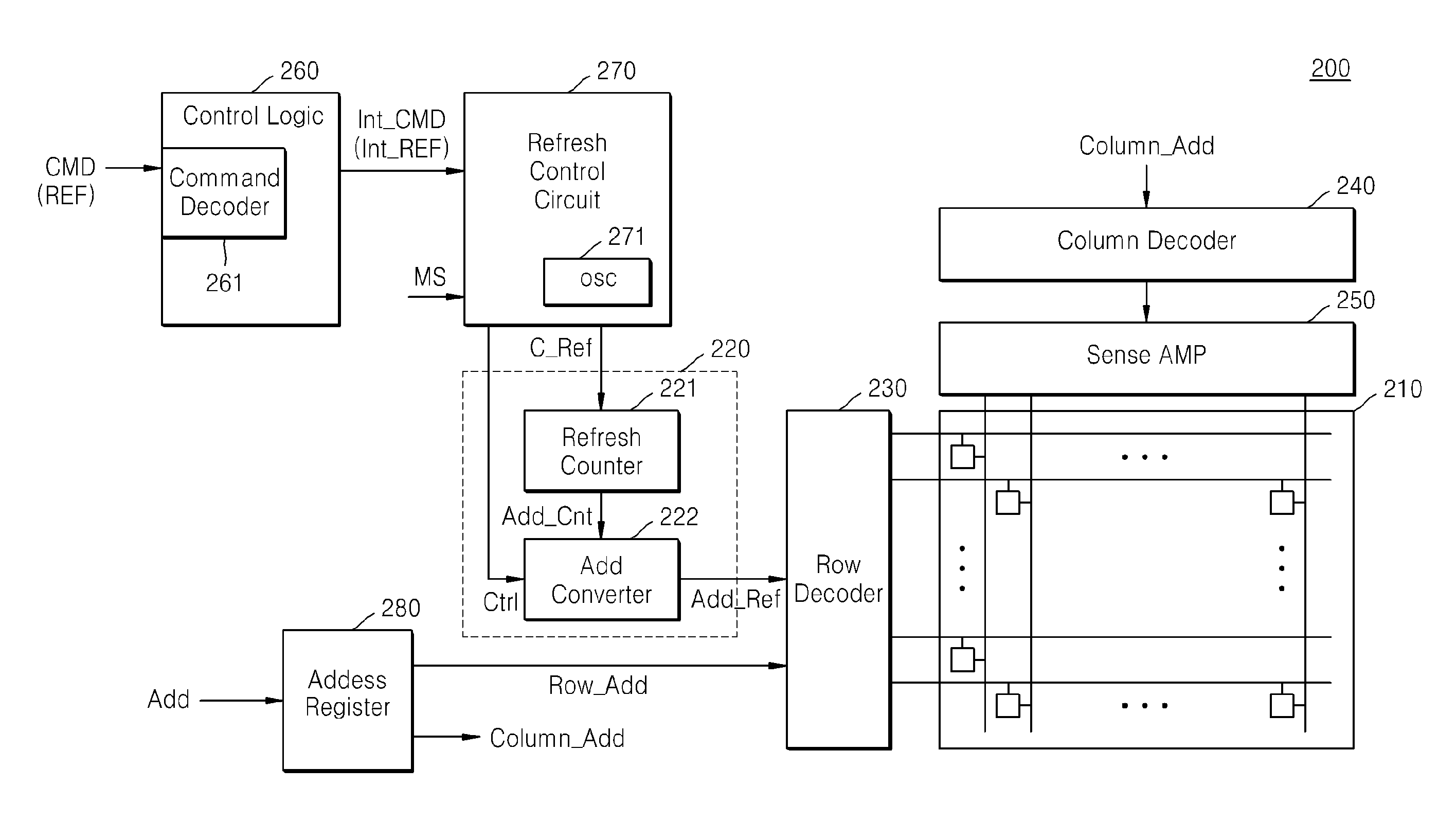
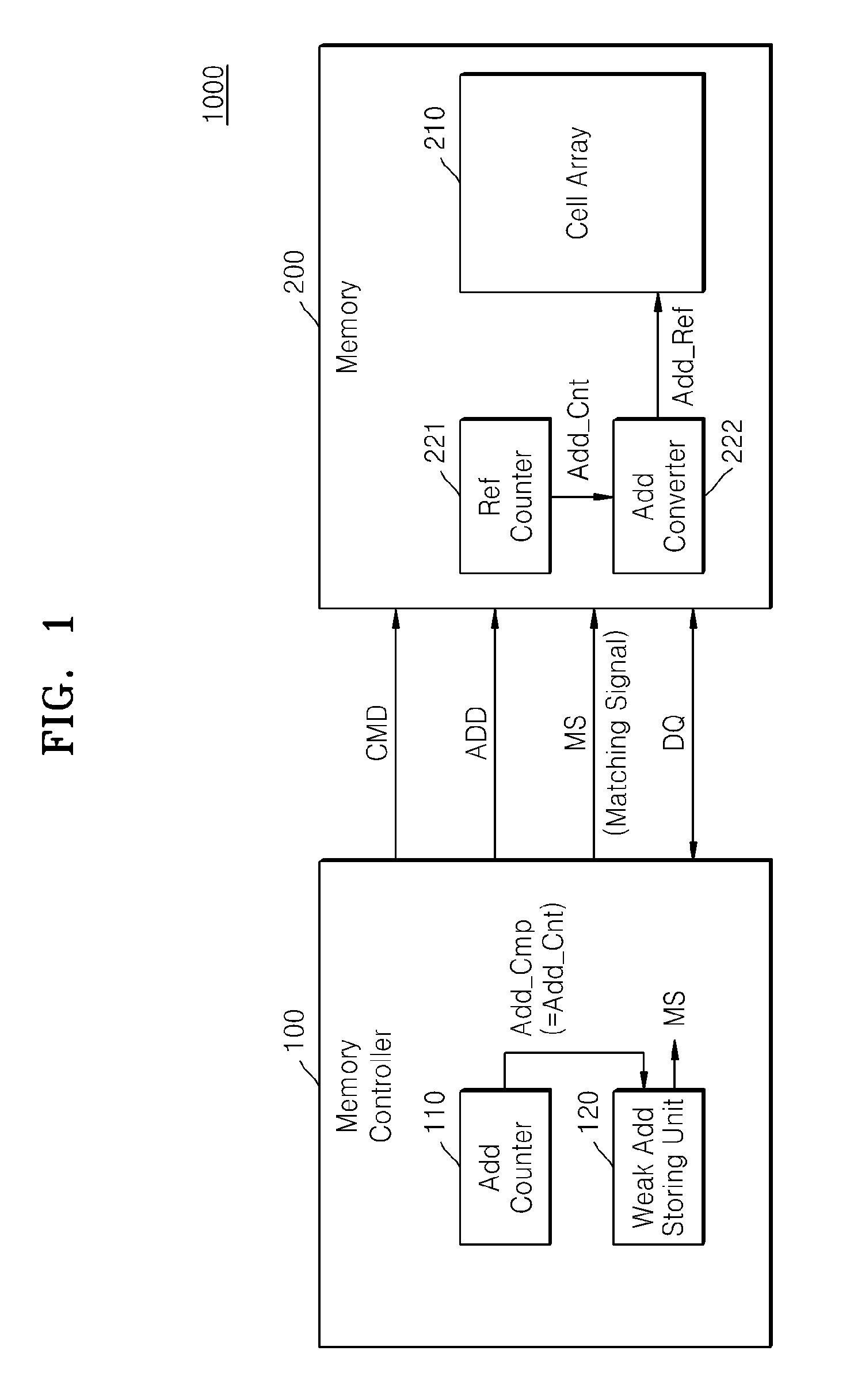
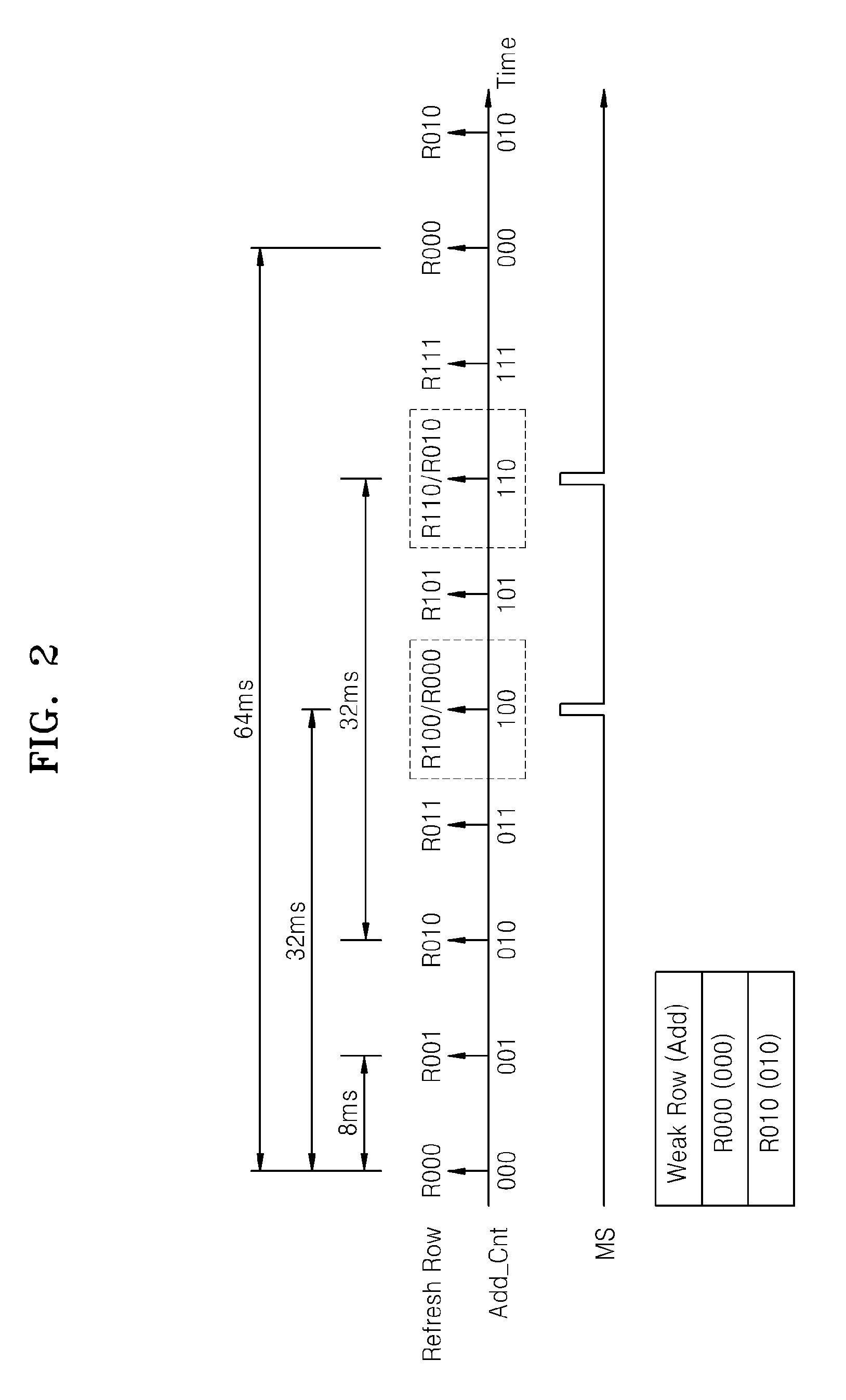
A semiconductor memory device includes a cell array including a plurality of cell regions, a row decoder configured to drive rows corresponding to cell regions in which a refresh operation is to be performed, based on a counting address, and a refresh address generator configured to generate the counting address and a modified address in response to a control signal, wherein the modified address is generated by inverting at least one bit of the counting address, and wherein the semiconductor memory device performs concurrent refresh operations on a first cell region corresponding to the counting address and a second cell region corresponding to the modified address where the second cell region is determined to have weak cells.

Description

CROSS-REFERENCE TO RELATED APPLICATIONS[0001]This application claims priority under 35 U.S.C. §119 to Korean Patent Application No. 10-2012-0105946 filed on Sep. 24, 2012, the disclosure of which is hereby incorporated by reference.BACKGROUND OF THE INVENTION[0002]The inventive concept relates generally to electronic memory technologies. More particularly, certain embodiments of the inventive concept relate to semiconductor memory devices having an adjustable refresh period.[0003]Certain types of memory devices require refresh operations to retain stored data. An example of such a memory device is a dynamic random access memory (DRAM), which stores data by maintaining charges in a capacitor. The charges tend to leak over time, so refresh operations are performed to compensate for this leakage. The refresh operation is typically performed on a periodic basis, with the period determined by the expected rate of charge leakage.[0004]In some contexts, the rate of charge leakage may vary ...

Claims


Application Information

Patent Timeline
Patent Type & Authority Patents(United States)
IPC IPC(8): G11C11/401G11C29/50G11C29/02G11C11/406G11C11/408G11C7/00G11C5/04G11C11/4076G06F12/00
CPCG11C7/00G11C11/408G11C11/4087G11C11/40611G11C11/40615G11C11/40622G11C29/023G11C29/028G11C29/50016G11C5/04G11C11/4076G11C2211/4065G11C2211/4068G11C11/406G11C11/4063
Inventor KANG, UK-SONG
Owner SAMSUNG ELECTRONICS CO LTD
Learn More