SIS semiconductor having junction barrier schottky device

a semiconductor and junction barrier technology, applied in the direction of semiconductor devices, basic electric elements, electrical appliances, etc., can solve the problem of difficult to effectively utilize the advantage of jbs structur

Active Publication Date: 2008-11-13
DENSO CORP
View PDF2 Cites 63 Cited by
  • Summary
  • Abstract
  • Description
  • Claims
  • Application Information

AI Technical Summary

Problems solved by technology

Therefore, it is difficult to provide ohmic contact with the P type layer, thereby, it is difficult to utilize the advantage of the JBS structure effectively.

Method used


Image

  • SIS semiconductor having junction barrier schottky device
  • SIS semiconductor having junction barrier schottky device
  • SIS semiconductor having junction barrier schottky device

Examples


first embodiment

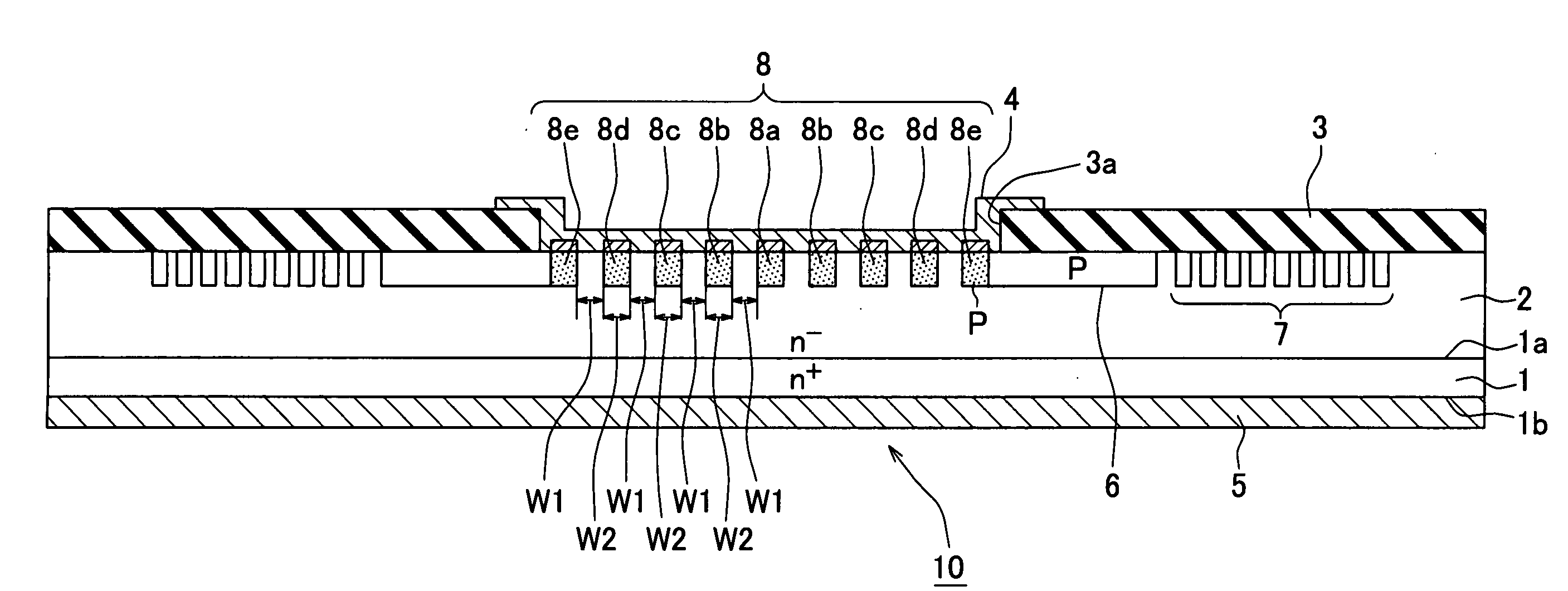
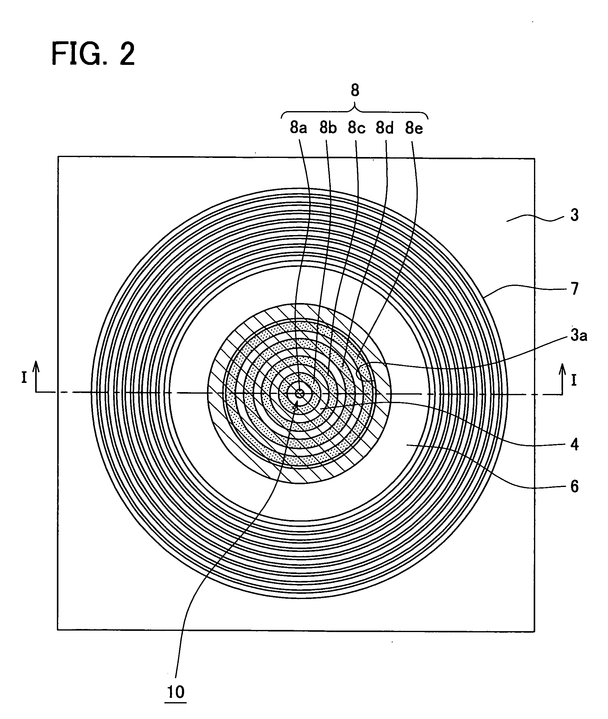
[0022]FIG. 1 is a cross sectional view showing a SiC semiconductor device having a JBS structure taken along line I-I in FIG. 2.

[0023]The SiC semiconductor device is made from a. N+ type substrate 1 made of SiC and having an impurity concentration, for example, in a range between 2×1018 cm−3 and 1×1021 cm−3. The substrate 1 has a principal surface 1a as an upper surface and a backside surface 1b as a lower surface, which is opposite to the principal surface 1a. On the principal surface 1a, a N− type drift layer 2 is stacked. The drift layer 2 is made of SiC and has an impurity concentration of 5×1015 cm−3 (±50%). A SBD structure 10 is formed in a cell region provided by the substrate 1 and the drift layer 2. A terminal structure is formed on an outer periphery region of the SBD structure 10. Thus, the semiconductor device includes the SBD structure 10 and the terminal structure.

[0024]Specifically, an insulation film 3 made of a silicon oxide film is formed on the surface of the drif...

second embodiment

[0039]FIG. 6 shows a SiC semiconductor device according to a second embodiment. The Schottky electrode 4 is formed of only one layer made of Mo, Ti or Ni. The impurity concentration profile of the P type layer 8 in FIG. 6 is different from that in FIG. 1, so that the P type layer 8 and the Schottky electrode 4 are coupled with the ohmic contact.

[0040]The impurity concentration of the surface portion of the P type layer 8 is higher than that of a deeper portion of the P type layer 8. For example, the surface portion of the P type layer 8, which contacts the Schottky electrode 4, has the P type impurity concentration equal to or higher than 1×1020 cm−3. Thus, the P type layer 8 and the Schottky electrode 4 are coupled with the ohmic contact. By increasing the impurity concentration of a contact portion of the P type layer 8 with the Schottky electrode 4, each of the Schottky diode property and the PN diode property effectively functions.

[0041]The manufacturing method of the device is ...

third embodiment

[0042]FIG. 7 shows a SiC semiconductor device having a JBS structure according to a third embodiment. The JBS structure and the outer periphery structure in FIG. 7 are different from those in FIG. 2. In FIG. 7, the RESURF layer 6 has a square shape with four rounded corners. The P type layer 8 including the center portion 8a and multiple ring portions 8b-8e has a square shape with four rounded corners. Specifically, the center portion 8a has the square shape with rounded corners, and each of the ring portions 8b-8e has the square shape with rounded corners, which surrounds the center portion 8a. The center portion 8a may be a circular shape.


PUM


Abstract

A semiconductor device having a junction barrier Schottky diode includes: a SiC substrate; a drift layer on the substrate; an insulation film on the drift layer having an opening in a cell region; a Schottky barrier diode having a Schottky electrode contacting the drift layer through the opening of the insulation film and an ohmic electrode on the substrate; a terminal structure having a RESURF layer surrounding the cell region; and multiple second conductive type layers on an inner side of the RESURF layer. The second conductive type layers and the drift layer provide a PN diode. The Schottky electrode includes a first Schottky electrode contacting the second conductive type layers with ohmic contact and a second Schottky electrode contacting the drift layer with Schottky contact.

Description

CROSS REFERENCE TO RELATED APPLICATION[0001]This application is based on Japanese Patent Application No. 2007-125593 filed on May 10, 2007, the disclosure of which is incorporated herein by reference. This application is also related to U.S. application Ser. No. ______, entitled “SIC SEMICONDUCTOR DEVICE HAVING JUNCTION BARRIER SCHOTTKY DIODE,” filed on ______.FIELD OF THE INVENTION[0002]The present invention relates to a SiC semiconductor device having a junction barrier Schottky diode.BACKGROUND OF THE INVENTION[0003]A Schottky barrier diode (i.e., SBD) includes a Schottky electrode, which contacts a semiconductor layer. An interface between the Schottky electrode and the semiconductor layer has a small work function between metallic material composing the Schottky electrode and semiconductor material composing the semiconductor layer. Accordingly, when a reverse voltage is applied to the diode, a leak current in the SBD is larger than a PN junction type diode.[0004]JP-2000-294804...

Claims


Application Information

Patent Timeline
Patent Type & Authority Applications(United States)
IPC IPC(8): H01L29/24
CPCH01L29/0615H01L29/0619H01L29/0692H01L29/1608H01L29/45H01L29/861H01L29/872
Inventor OKUNO, EIICHIYAMAMOTO, TAKEO
Owner DENSO CORP
Why Eureka
Try Eureka