Schottky barrier diode and diode array

a technology of diodes and arrays, applied in the direction of diodes, semiconductor devices, semiconductor/solid-state device details, etc., can solve the problems of small chip area and low resistance of schottky barrier diodes, and achieve the effect of small chip area and low on resistan

Active Publication Date: 2006-05-25
PANASONIC CORP
View PDF4 Cites 58 Cited by
  • Summary
  • Abstract
  • Description
  • Claims
  • Application Information

AI Technical Summary

Benefits of technology

[0035] As described above, in the Schottky barrier diode and the diode array of this inve

Problems solved by technology

As a result, the Schottky barrier diode attain

Method used


Image

  • Schottky barrier diode and diode array
  • Schottky barrier diode and diode array
  • Schottky barrier diode and diode array

Examples


embodiment 1

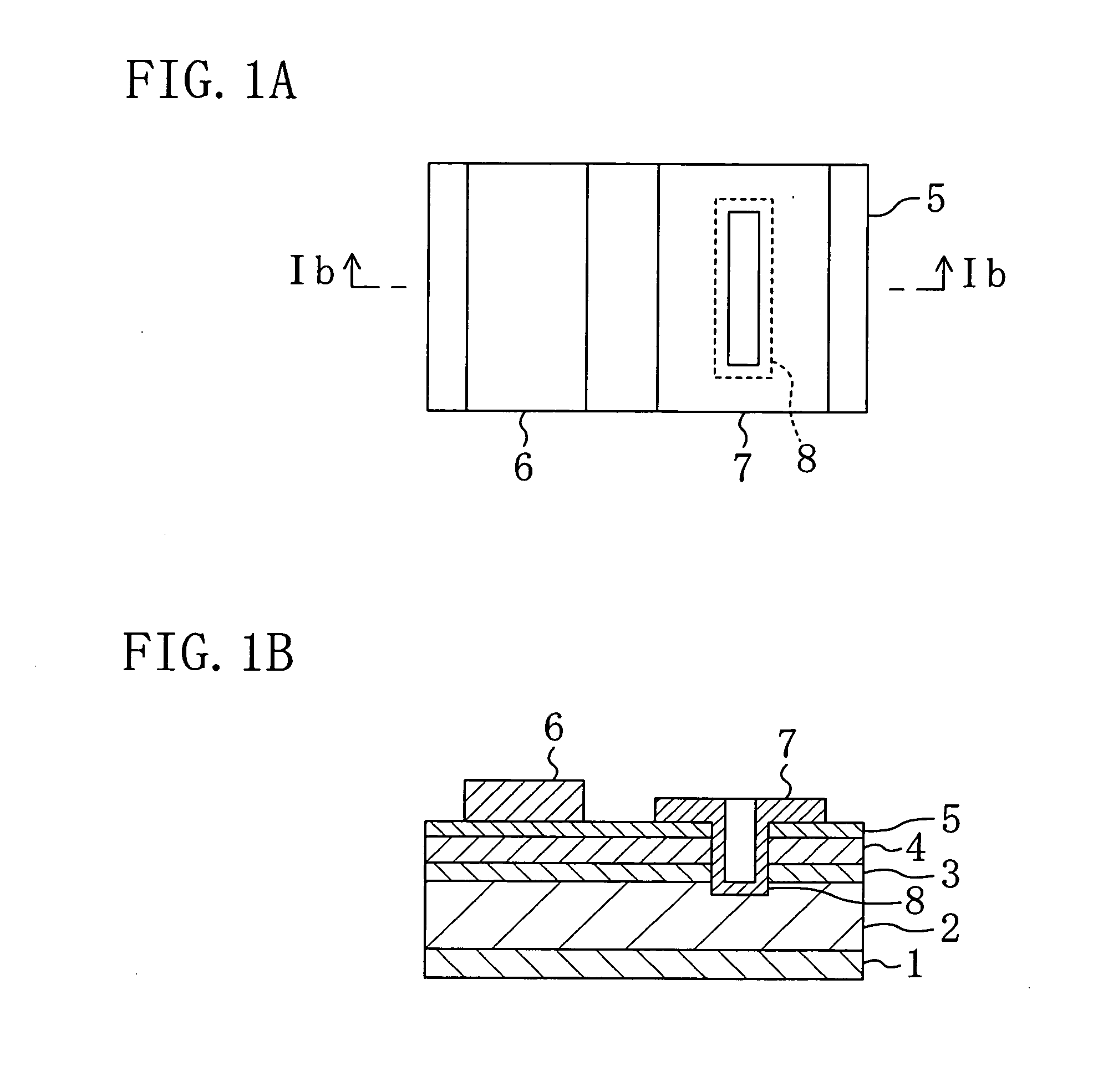
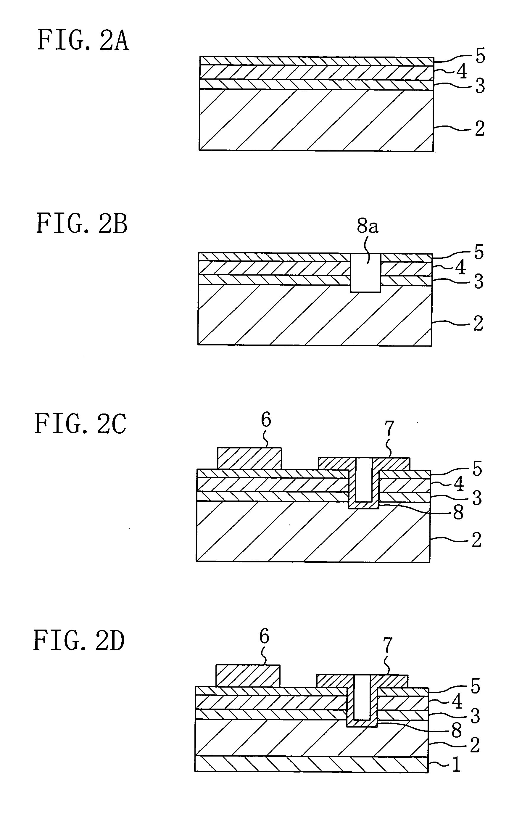
[0054]FIGS. 1A and 1B show the structure of a Schottky barrier diode (SBD) of Embodiment 1 of the invention, and specifically, FIG. 1A is a plan view thereof and FIG. 1B is a cross-sectional view thereof taken on line Ib-Ib of FIG. 1A.

[0055] As shown in FIG. 1B, a buffer layer 3 of aluminum nitride (AlN) with a thickness of 100 nm is formed on a conductive n-type silicon (n+-Si) substrate 2. The buffer layer 3 has very high resistance because it includes a large number of crystal defects derived from a difference in the lattice constant between the crystal of the buffer layer 3 and the crystal of the n+-Si substrate 2.

[0056] A first semiconductor layer 4 of undoped gallium nitride (GaN) is formed on the buffer layer 3, and a second semiconductor layer 5 of undoped aluminum gallium nitride (Al0.26Ga0.74N) is deposited on the first semiconductor layer 4 by metal organic chemical vapor deposition (MOCVD). On an interface in the first semiconductor layer 4 between the first semiconduc...

modification 1

OF EMBODIMENT 1

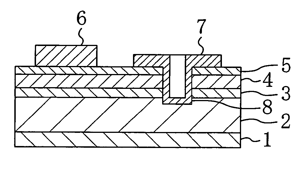
[0068]FIG. 3 shows the structure of an SBD according to Modification 1 of Embodiment 1 of the invention. In FIG. 3, like reference numerals are used to refer to like elements shown in FIGS. 1A and 1B so as to omit the description. As shown in FIG. 3, the SBD of this modification includes a via 8 penetrating through a substrate 2, and an ohmic electrode 7 and a back face electrode 1 are directly electrically connected to each other through the via 8.

[0069] Although it is necessary to form a via hole penetrating through the substrate 2 in the SBD of this modification, the on resistance can be further lowered than in the SBD of Embodiment 1 because no current flows in the substrate 2.

modification 2

OF EMBODIMENT 1

[0070]FIG. 4 shows the structure of an SBD according to Modification 2 of Embodiment 1 of the invention. In FIG. 4, like reference numerals are used to refer to like elements shown in FIGS. 1A and 1B so as to omit the description. As shown in FIG. 4, the SBD of this modification includes a Schottky electrode 6 connected to a substrate 2 through a via 8, and the Schottky electrode 6 is drawn to the back face. Also, an insulating film 9 of silicon nitride (SiN) is formed on the inner wall of a via hole 8a for preventing electric short-circuit between the via 8 and the 2DEG.

[0071] Since the Schottky electrode 6 is connected to the back face electrode in the SBD of this modification, when a backward bias voltage is applied, a depletion layer extends not only from the Schottky electrode 6 but also from the substrate 2, and hence, the electric field concentration can be avoided, resulting in increasing the breakdown voltage of the SBD.

EMBODIMENT 2

[0072] An SBD according ...


PUM


Abstract

A Schottky barrier diode includes a first semiconductor layer and a second semiconductor layer successively formed above a semiconductor substrate with a buffer layer formed between the first and second semiconductor layers and the semiconductor substrate. A Schottky electrode and an ohmic electrode spaced from each other are formed on the second semiconductor layer, and a back face electrode is formed on the back face of the semiconductor substrate. The Schottky electrode or the ohmic electrode is electrically connected to the back face electrode through a via penetrating through at least the buffer layer.

Description

CROSS-REFERENCE TO RELATED APPLICATIONS [0001] This application claims priority under 35 U.S.C. § 119 on Patent Application No. 2004-340531 filed in Japan on Nov. 25, 2004, the entire contents of which are hereby incorporated by reference. BACKGROUND OF THE INVENTION [0002] The present invention relates to a Schottky barrier diode and a diode array, and more particularly, it relates to a Schottky barrier diode and a diode array using a two-dimensional electron gas. [0003] A Schottky barrier diode (SBD) is required to have a high breakdown voltage and low on resistance. In order to realize a high breakdown voltage in a conventional SBD using a silicon (Si) material, the thickness of a drift layer where a depletion layer extends in applying a backward bias voltage is increased and a carrier concentration is lowered. The drift layer is, however, a region where electrons pass in applying a forward bias voltage, and hence, the on resistance of the SBD is increased when the thickness of t...

Claims


Application Information

Patent Timeline
IPC IPC(8): H01L31/07H01L21/3205H01L21/329H01L21/768H01L21/822H01L23/522H01L27/04H01L29/41H01L29/47H01L29/872
CPCH01L21/26506H01L27/0605H01L27/0814H01L29/0692H01L29/417H01L29/66143H01L29/872
Inventor YANAGIHARA, MANABUUEMOTO, YASUHIROTANAKA, TSUYOSHIUEDA, DAISUKE
Owner PANASONIC CORP
Why Eureka
Try Eureka