Semiconductor device

a technology of schottky barrier and semiconductor, which is applied in the direction of electric variable regulation, process and machine control, instruments, etc., can solve the problems of reducing unable to achieve sufficient effect, and commutating the load current to the schottky barrier diode, so as to reduce the inductance of the wiring section, reduce the diode conduction loss and the effect of diode recovery loss

Inactive Publication Date: 2005-10-20
RENESAS ELECTRONICS CORP
View PDF2 Cites 59 Cited by
  • Summary
  • Abstract
  • Description
  • Claims
  • Application Information

AI Technical Summary

Benefits of technology

[0015] Advantageous effects obtained by the present invention as disclosed in the present application will be explained in brief as follows:
[0016] The first field effect transistor, the second field effect transistor, the control circuit and the Schottky barrier diode are respectively formed in discrete semiconductor chips, and the discrete semiconductor chips are encapsulated in one sealing body. Consequently, a wiring section that electrically connects th...

Problems solved by technology

That is, with a construction in which several packages are provided, problems result in that the commutation of a load current to the Schottky barrier diode during the dead time is impaired by the inductances of a wiring for electrically connecting the cathode of the Schottky barrier diode and the output of the DC-DC converter and a wiring for electrically connecting the anode of the Schottky barrier diode and a ground wiring, so that despite the use of a Schottky barrier diode having a lower forward voltage than that of the parasitic diode, a sufficient effect cannot be obtained in terms of a reduction in diode conduction loss and a reduction in diode recovery loss due to the reverse recovery time being made fast.
A problem arises in that, when the load current that flows through the Schottky barrier diode during the dead time becomes small due to the wiring inductances and the load current flows even into the body diode of the power MOS·FET for the lowside switch, the potential on the output side of the DC-DC converter is reduced to a negative potential by the forward voltage of the body d...

Method used


Image

  • Semiconductor device
  • Semiconductor device
  • Semiconductor device

Examples


first preferred embodiment

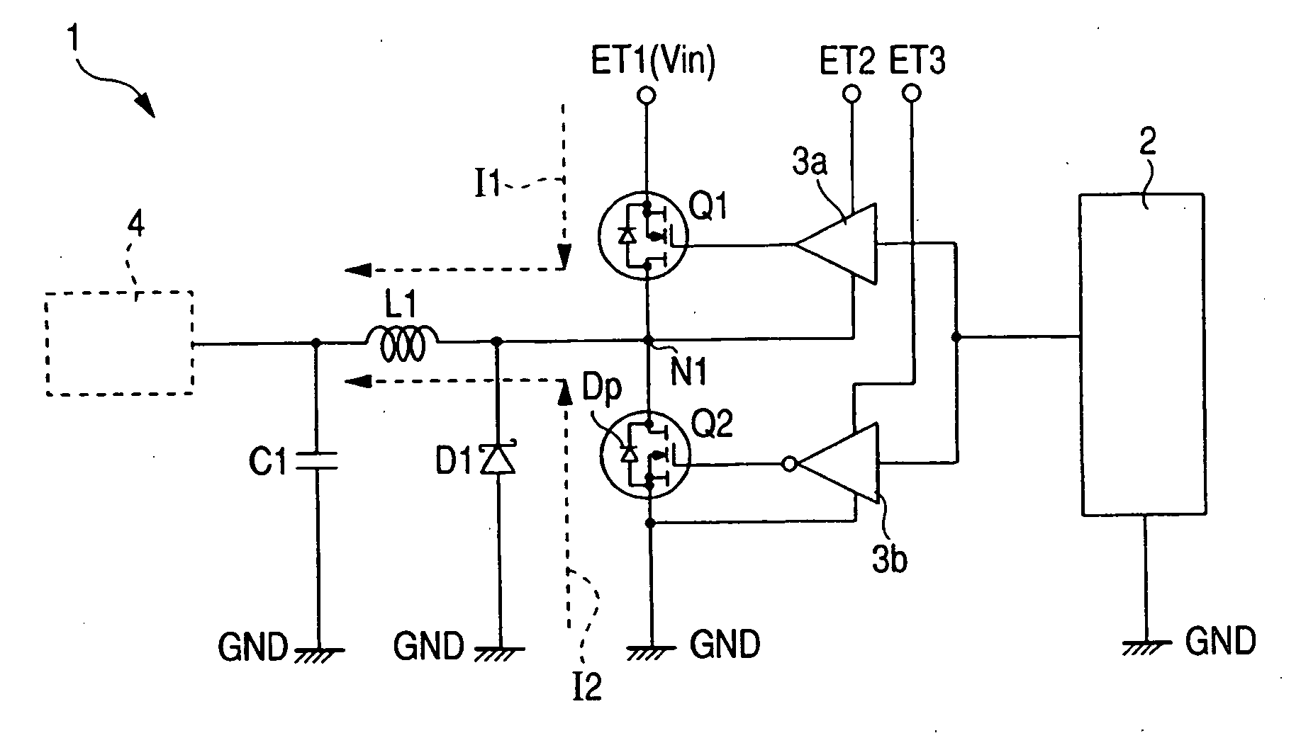
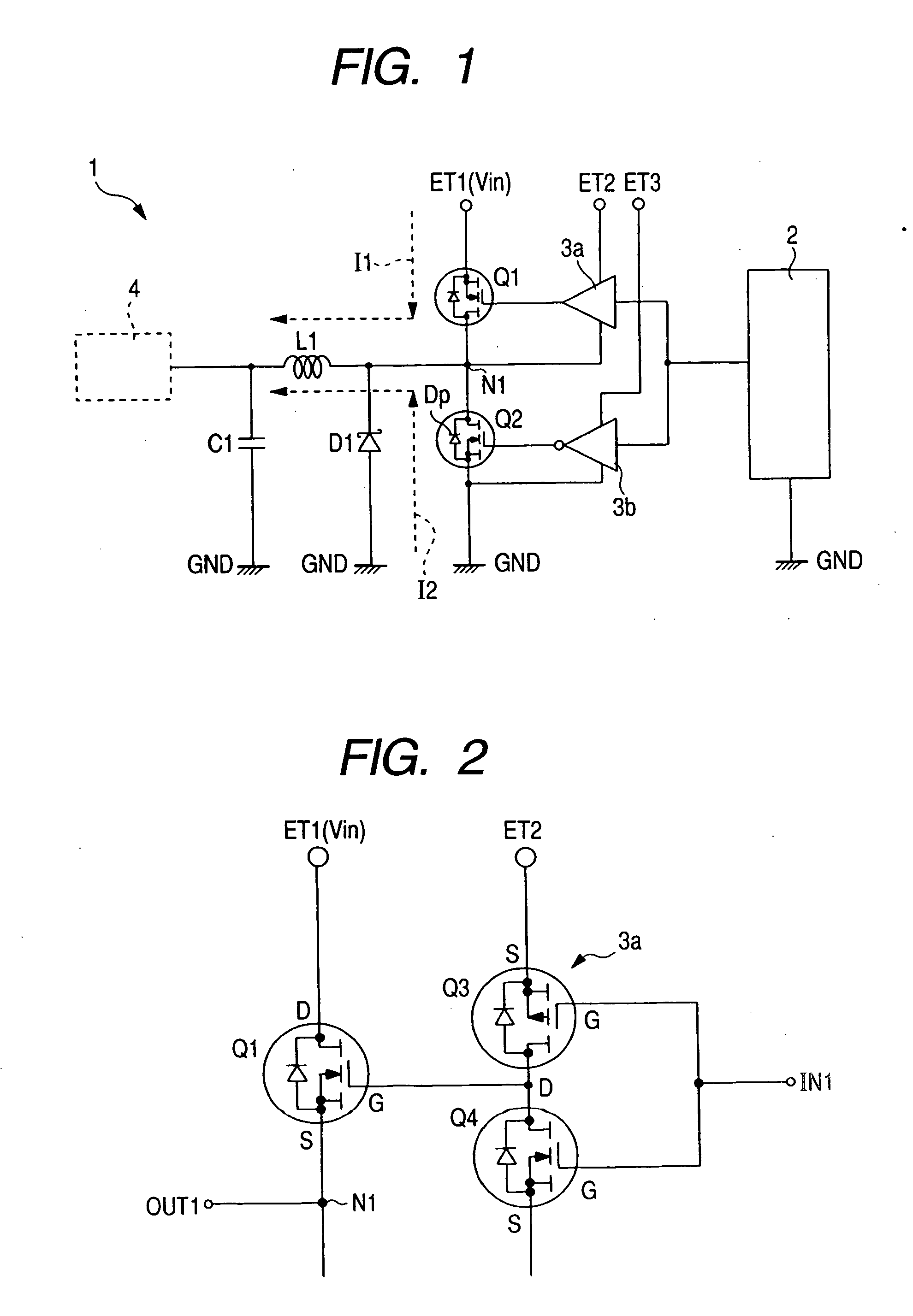
[0073] A semiconductor device according to a first embodiment of the present invention operates as a non-insulated DC-DC converter of the type used in a power supply circuit of an electronic apparatus like, for example, a desk top personal computer, a notebook-size personal computer, a server or a game machine or the like. FIG. 1 shows one example of a circuit diagram of the non-insulated DC-DC converter 1. The non-insulated DC-DC converter 1 includes a control circuit 2, driver circuits (first and second control circuits) 3a and 3b, power MOSs (first and second field effect transistors) Q1 and Q2, a Schottky barrier diode (first diode) D1, a coil L1 and a capacitor C1, etc.

[0074] The control circuit 2 is a circuit which supplies a signal for controlling the voltage switch-on widths (on time) of the power MOSs Q1 and Q2. The control circuit 2 is packaged aside from the power MOSs Q1 and Q2. The output (corresponding to a terminal for the control signal) of the control circuit 2 is ...

second preferred embodiment

[0145]FIG. 31 is a plan view showing an example of a package 6 according to a second embodiment, FIG. 32 is a plan view showing an example of the package 6 except for metal plate wirings of FIG. 31, FIG. 33 is a cross-sectional view taken along line Y3-Y3 of FIG. 31, and FIG. 34 is a cross-sectional view taken along line X3-X3 of FIG. 31. Incidentally, FIGS. 31 and 32 also show a sealing member MB as seen therethrough to make it easy to see the elements in the drawings. Further, die pads 7a1 and 7a2, leads 7b and a wiring section 7c are given hatching.

[0146] In the second embodiment, some of wirings for electrically connecting pads and respective portions are configured as metal plate wirings 36 in place of wires. That is, pads BP1 for a source electrode of a power MOS Q1 of a semiconductor chip 5a are electrically connected to a die pad 7a2 through one metal plate wiring 36. A BP5 for a source electrode of a power MOS Q2 of a semiconductor chip 5b is electrically connected to lead...

third preferred embodiment

[0151]FIG. 35 is a plan view showing a top surface of a package 6 according to a third embodiment, and FIGS. 36 and 37 are, respectively, cross-sectional views taken along line Y4-Y4 of FIG. 35 and line X4-X4 thereof. Incidentally, the arrangement of the inside of the package 6 is identical to that shown in FIG. 31. In FIG. 35, the top surface of the package 6 is given hatching to make it easy to see in the drawing. The top surface of the package 6 corresponds to a surface lying on the side opposite to a mounting surface (surface opposite to a wiring board) of the package 6.

[0152] In the third embodiment, the pads and respective portions are connected by metal plate wirings 36 in a manner similar to the second embodiment. However, some of the metal plate wirings 36 are exposed from a resin molded body MB. The metal plate wirings 36 are disposed so as to cover regions for forming power MOSs Q1 and Q2 corresponding to heat generation sources of semiconductor chips 5a and 5b. The pres...


PUM


Abstract

A non-insulated DC-DC converter a power MOS·FRT for a highside switch and a power MOS·FET for a lowside switch. In the non-insulated DC-DC converter, the power MOS·FET for the highside switch and the power MOS·FET for the lowside switch, driver circuits that control operations of these elements, respectively, and a Schottky barrier diode connected in parallel with the power MOS·FET for the lowside switch are respectively formed in four different semiconductor chips. These four semiconductor chips are housed in one package. The semiconductor chips are mounted over the same die pad. The semiconductor chips are disposed so as to approach each other.

Description

[0001] CROSS-REFERENCE TO RELATED APPLICATION [0002] The present application claims priority from Japanese patent application No. 2004-123153, filed on Apr. 19, 2004, the content of which is hereby incorporated by reference into this application. BACKGROUND OF THE INVENTION [0003] The present invention relates in general to a semiconductor device, and, more particularly, to a technique that is effective when applied to a semiconductor device having a power supply circuit. [0004] A DC-DC converter, which is widely used as one example of a power supply circuit, has a configuration wherein a power MOS·FET (Metal Oxide Semiconductor Field Effect Transistor) for a highside switch and a power MOS·FET for a lowside switch are connected in series. The power MOS·FET for the highside switch has a switch function for control of the DC-DC converter. The power MOS·FET for the lowside switch has a switch function for synchronization and rectification. The conversion of a power supply voltage is p...

Claims


Application Information

Patent Timeline
IPC IPC(8): H01L25/07H01L21/8238H01L25/04H01L25/18H01L27/092H01L29/06H01L29/78H02M1/08H02M3/155H02M7/217
CPCH01L24/34H01L2224/49175H01L2224/48091H01L2224/48137H01L2224/48247H01L2224/49H01L2924/01004H01L2924/01013H01L2924/01029H01L2924/01033H01L2924/01047H01L2924/0105H01L2924/01057H01L2924/01059H01L2924/01079H01L2924/01082H02M1/08H01L24/49H01L2224/49171H01L2224/40247H01L2924/01005H01L2924/01006H01L2924/01023H01L2924/01074H01L2924/014H01L2924/13091H01L2924/1305H01L2224/45144H01L2924/12032H01L2924/1306H01L2924/3011H01L2224/40137H01L2924/30107H01L2224/73221H01L2924/00014H01L2924/00H01L2924/181H01L2224/40095H01L24/40H01L2224/40245H01L2224/05599H01L2224/45015H01L2224/85444H01L24/48H01L2924/14H01L2224/0603H01L24/45H01L2224/05554H01L2224/371H01L24/37H01L2224/37124H01L2224/37147H01L2224/83801H01L2224/8485H01L2224/84801H01L24/84H01L2924/00012H01L2924/20753H01H9/02
Inventor UNO, TOMOAKISHIRAISHI, MASAKIMATSUURA, NOBUYOSHINAGASAWA, TOSHIO
Owner RENESAS ELECTRONICS CORP
Why Eureka
Try Eureka