Organic semiconductor diode

a semiconductor diode and organic technology, applied in the field of organic semiconductor diodes, can solve the problems of low electric conductivity value of organic compounds used in said diodes, relatively expensive production process, and low cost advantage of vacuum processes

Inactive Publication Date: 2007-05-01
NITTO DENKO CORP
View PDF6 Cites 58 Cited by
  • Summary
  • Abstract
  • Description
  • Claims
  • Application Information

AI Technical Summary

Problems solved by technology

In addition, organic compounds used in said diodes have low values of the electric conductivity.
Furthermore, the organic layers of organic diodes have been manufactured in relatively expensive production process.
These vacuum processes do not create cost advantage that would be expected from introduction of a new material in well known function.
Another disadvantage of the aforementioned organic diodes is low temperature stability of the organic material itself.
The desirable temperature range for diode operation in many applications is between −40 and 700° C. Present organic diodes do not satisfactorily meet these temperature requirements.

Method used


Image

  • Organic semiconductor diode
  • Organic semiconductor diode
  • Organic semiconductor diode

Examples


example 1

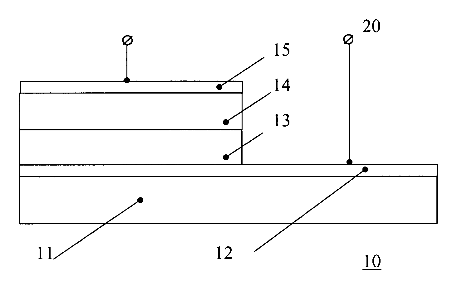
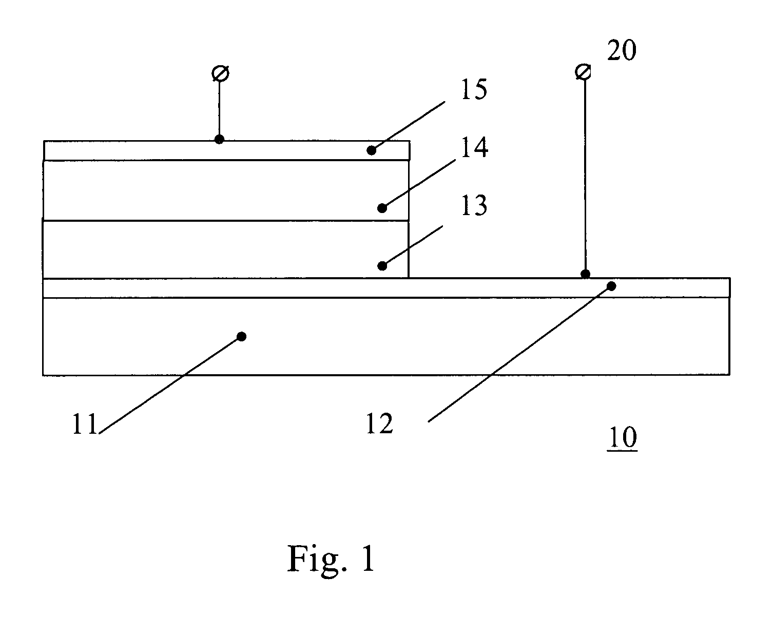
[0121]The organic semiconductor diodes with the p-n junction were prepared as follows. Thin films of materials specified below were sequentially applied onto a glass substrate. First, an ITO film with a thickness of 1100 Å was formed by vacuum deposition at a pressure of 5.0×10⁻⁶ Torr to serve as the anode. Then, a thin film of a sulfoderivative of copper phthalocyanines with the structural formula XXIV was formed on the ITO layer by method of Cascade Crystallization Process to serve as the hole transport layer. The thickness of this layer was 0.3 μm. Next, a thin film of a perylene derivative with the formula (Ia) was formed over the hole transport layer by method of Cascade Crystallization Process to serve as the electron transport layer. The thickness of the electron transport layer was also 0.3 μm. Further, a thin film of lithium oxide (LiO2) was deposited onto the electron transport layer at a rate of 1 Å / sec to serve as the cathode. The LiO2 layer thickness was 0.5 nm. Finally...

example 2

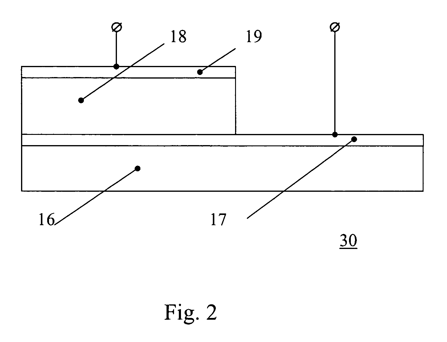
[0122]The organic semiconductor diode with the p-n junction was prepared similarly to the diode described in Example 1, except that perylene derivatives represented by the formula (Va)

[0123]

was used as material for the electron transport layer.

example 3

[0124]The organic semiconductor diode with the p-n junction was prepared similarly to the diode described in Example 1, except that perylene derivatives represented by the formula (Vb)

[0125]

was used as material for the electron transport layer.


PUM


Abstract

The present invention relates to organic semiconductor diodes, in particular, to the diodes with nonlinear current-voltage characteristics, which are used for power switching, rectifying variable signals, and frequency mixing. The organic semiconductor diode with the p-n junction comprises an anode, cathode, a hole transport layer in contact with the anode, and an electron transport layer in contact with the cathode, and two transport layers being in contact with each other. Another aspect of the present invention is a Schottky barrier diode comprising anode, cathode, and an organic semiconductor layer, wherein the semiconductor layer is either hole or electron transport layer. At least one of the transport layers is characterized by a globally ordered crystalline structure with intermolecular spacing of 3.4±0.3 Å in the direction of one crystal axis. One more aspect of the present invention is a method for obtaining an organic semiconductor layer with the electron-hole type of conductivity.

Description

FIELD OF THE INVENTION[0001]The present invention relates to semiconductor diodes, and more particularly to semiconductor diodes using organic materials.BACKGROUND OF THE INVENTION[0002]An organic diode has been fabricated which makes use of the electrical conductivity of a low-density polyethylene (LDPE) [L. Boundou, J. Guastavino, N. Zouzou, and J. Martinez Vega, Influence of Annealing Treatment on the Electrical Conductivity of Low Density Polyethylene, Polymer International, 50(9), 1046–1049 (2001), incorporated herein by reference]. This paper reports on the conductivity of semicrystalline, additive free (undoped) low-density polyethylene (LDPE) samples in the form of 100 μm thick discs prepared from hot pressed LDPE pellets. Both faces of each sample were coated with gold by vacuum deposition. The samples were studied by measuring the current through the structure during a stepwise increase in the applied voltage (i.e., in the electric field) at various temperatures. The resul...

Claims


Application Information

Patent Timeline
Patent Type & Authority Patents(United States)
IPC IPC(8): H01L29/47H01L51/30
CPCH01L51/0053H01L51/0583H01L51/105H01L51/0078H10K85/621H10K85/311H10K10/26H10K10/84
Inventor LAZAREV, PAVEL I.
Owner NITTO DENKO CORP
Why Eureka
Try Eureka