Semiconductor device having schottky junction electrode

a technology of schottky junction and semiconductor, which is applied in the direction of semiconductor devices, semiconductor/solid-state device details, electrical apparatus, etc., can solve the problems of destabilizing element charact and thermal instability of the barrier, and achieve excellent power performance and reliability, improve the heat resistance of the schottky junction electrode, and improve the effect of the heat resistan

Inactive Publication Date: 2005-07-14
NEC CORP
View PDF4 Cites 62 Cited by
  • Summary
  • Abstract
  • Description
  • Claims
  • Application Information

AI Technical Summary

Benefits of technology

[0008] The present invention has been created in light of the afore-mentioned problems of the prior art. Therefore, the purpose of the present invention is to improve the heat resistance of the Schottky junction electrode and to provide a semiconductor device using GaN, which has excellent power performance and reliability, as principal material. The first aspect of the present invention is a semiconductor device containing a semiconductor layer comprising a compound semiconductor, which uses GavAl1−v (where, 0≦v≦1) as the main constituent of the Group III-element and N as the main constituent of the Group V-elements, and a Schottky junction metal layer which is in contact with the semiconductor layer. In this semiconductor device, the Schottky junction metal layer comprises a laminated structure containing a first metal layer contacting the semiconductor layer, a second met

Problems solved by technology

If the Schottky junction electrode 67 comprises Ni, Pt and Pd, even though a high Schottky barrier can be obtained, a problem exists in that the barrier is thermally unstable, such as the transposition point of Ni being low, approximately 353° C., for exampl

Method used


Image

  • Semiconductor device having schottky junction electrode
  • Semiconductor device having schottky junction electrode
  • Semiconductor device having schottky junction electrode

Examples


first embodiment

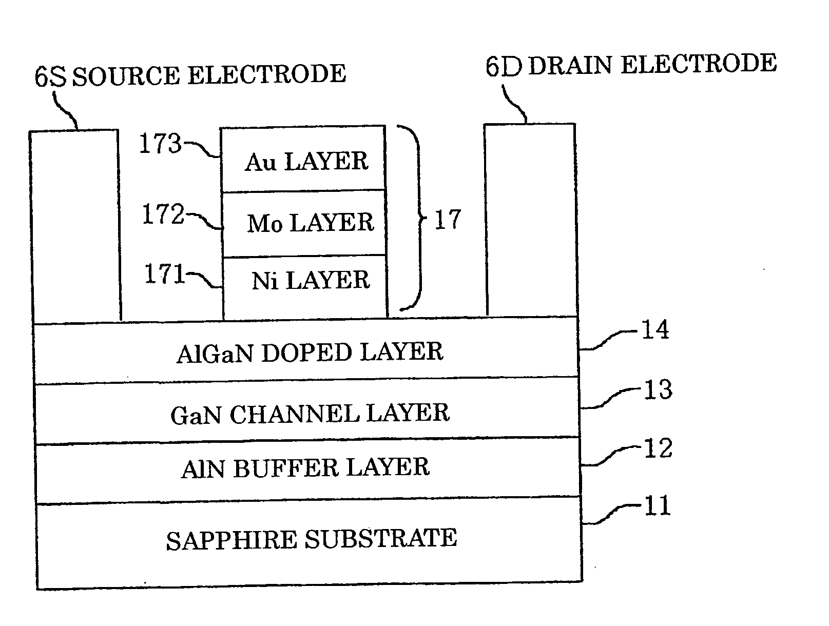
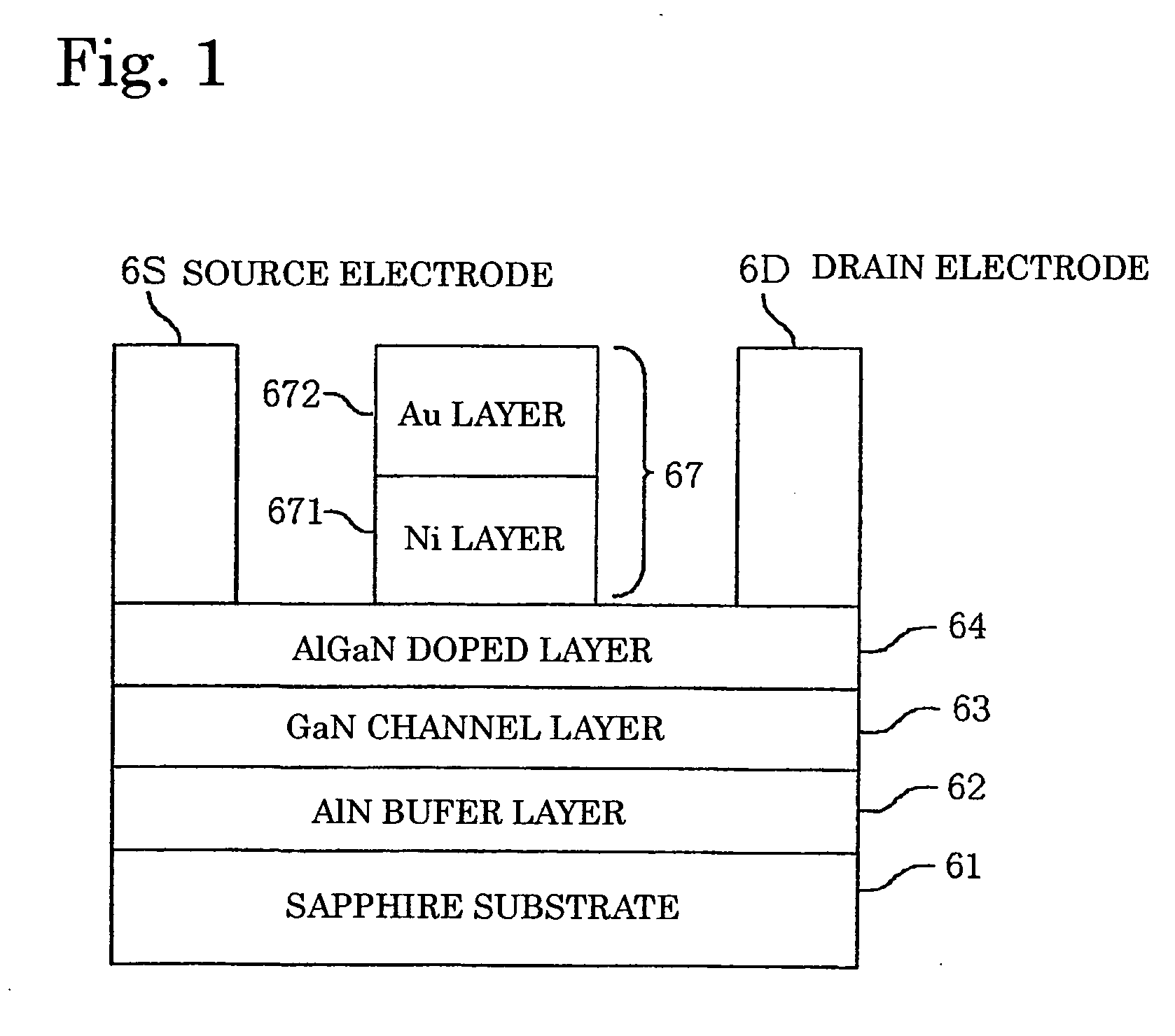
[0053] Described is a first embodiment according to the present invention in reference to FIG. 5, FIG. 6, and FIG. 7.

[0054]FIG. 5 is a local longitudinal sectional view showing the main structure of an AlGaN / GaN heterojunction field-effect transistor (HJFET) in the first embodiment according to the present invention. The transistor is formed on a sapphire substrate 11. In FIG. 5, an undoped AlN buffer layer 12 is formed on the sapphire substrate 11. An undoped GaN channel layer 13 is formed on the undoped AlN buffer layer 12. An undoped AlGaN electron supplying layer 14 is formed on the undoped GaN channel layer 13. Furthermore, a source electrode 6S and a drain electrode 6D are formed in contact with the upper surface of the AlGaN electron supplying layer 14. The source electrode 6s and the drain electrode 6D are in ohmic contact with the AlGaN electron supplying layer 14.

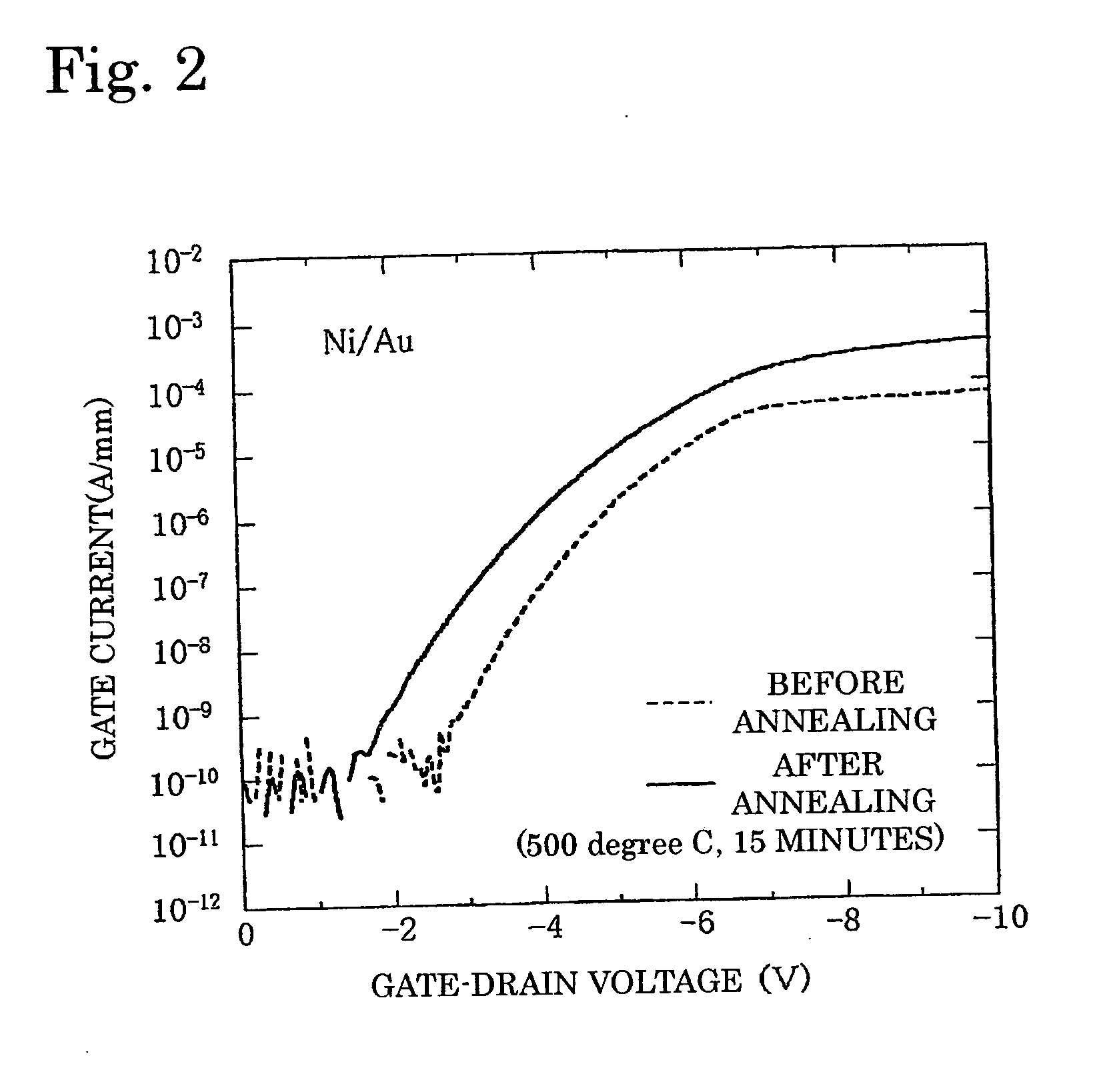
[0055] Furthermore, a gate electrode 17 is formed in contact with the upper surface of the AlGaN electron sup...

second embodiment

[0067] Next, a second embodiment according to the present invention is described in reference to FIG. 8.

[0068]FIG. 8 is a local vertical view showing the main structure of an AlGaN / GaN heterojunction field-effect transistor (HJFET) in the second embodiment according to the present invention. The transistor is formed on a sapphire substrate 21. In FIG. 8, an undoped AlN buffer layer 22 with a film thickness of 20 nm is formed on the sapphire substrate 21, an undoped GaN channel layer 23 with a film thickness of 2 μm is formed on the AlN buffer layer 22, and an AlGaN electron supplying layer 24 comprising undoped Al0.3Ga0.7N with a film thickness of 30 nm is formed on the GaN channel layer 23.

[0069] A source electrode 6S and a drain electrode 6D are formed in contact with the upper surface of the AlGaN electron supplying layer 24. The source electrode 6S and the drain electrode 6D are in ohmic contact with the AlGaN electron supplying layer 24. Furthermore, a gate electrode 27 is fo...

third embodiment

[0076] Next, a third embodiment according to the present invention is described in reference to FIG. 9.

[0077]FIG. 9 is a local vertical view showing the main structure of an AlGaN / GaN heterojunction field-effect transistor (HJFET) in the third embodiment according to the present invention. The transistor is formed on a SiC substrate 31. In FIG. 9, an undoped AlN buffer layer 32 is formed on the SiC substrate 31, an undoped GaN buffer layer 33 with a film thickness of 2 μm is formed on the undoped AlN buffer layer 32, an InGaN channel layer 34 comprising an undoped In0.1Ga0.9N with a film thickness of 15 nm is formed on the undoped GaN buffer layer 33, and an AlGaN electron supplying layer 35 comprising an undoped Al0.2Ga0.8N with a film thickness of 40 nm is formed on the InGaN channel layer 34.

[0078] A source electrode 6S and a drain electrode 6D are formed in contact with the upper surface of the AlGaN electron supplying layer 35. The source electrode 6S and the drain electrode ...


PUM


Abstract

A GaN semiconductor device with improved heat resistance of the Schottky junction electrode and excellent power performance and reliability is provided. In this semiconductor device having a Schottky gate electrode 17 which is in contact with an AlGaN electron supplying layer 14, a gate electrode 17 comprises a laminated structure wherein a first metal layer 171 formed of any of Ni, Pt and Pd, a second metal layer 172 formed of any of Mo, Pt, W, Ti, Ta, MoSi, PtSi, WSi, TiSi, TaSi, MoN, WN, TiN and TaN, and a third metal layer formed of any of Au, Cu, Al and Pt. Since the second metal layer comprises a metal material having a high melting point, it works as a barrier to the interdiffusion between the first metal layer and the third metal layer, and the deterioration of the gate characteristics caused by high temperature operation is suppressed. Since the first metal layer contacting the AlGaN electron supplying layer 14 has a high work function, the Schottky barrier is high, and superior Schottky contact is obtained.

Description

TECHNICAL FIELD [0001] The present invention relates to a high output semiconductor device used in a microwave band comprising GaN as the principal material. Particularly, the present invention relates to a Schottky junction electrode used for a semiconductor device superior in heat resistance and power performance. [0002] In order to more sufficiently describe the current level of technology pertaining to the present invention, all descriptions of the patents, the patent applications, the patent publications, the treatises on science or the like that are cited or specified in the present patent application are incorporated hereinto through reference. Background of the Art [0003]FIG. 1 is a local longitudinal sectional view of a semiconductor device having a conventional Schottky junction electrode. The semiconductor device is reported, for example, in the Reference, IEEE Trans. Microwave Theory Tech. (Vol. No. 46, No. 6, Page 756, 1998) authored by U. K. Mishra et al. [0004] As sh...

Claims


Application Information

Patent Timeline
IPC IPC(8): H01L21/338H01L29/872H01L29/20H01L29/423H01L29/47H01L29/778H01L29/812
CPCH01L29/2003H01L29/7787H01L29/475H01L29/7781H01L29/812
Inventor ANDO, YUJIMIYAMOTO, HIRONOBUOKAMOTO, YASUHIROKASAHARA, KENSUKENAKAYAMA, TATSUOKUZUHARA, MASAAKI
Owner NEC CORP
Why Eureka
Try Eureka