Vertical Super-Thin Body Semiconductor on Dielectric Wall Devices and Methods of Their Fabrication

a dielectric wall and semiconductor technology, applied in semiconductor devices, semiconductor/solid-state device details, electrical apparatus, etc., can solve the problems of unmanufacturability of finfet on soi, inability to manufacture super-thin body on soi with a required uniformity across a 300 mm (or 450 mm in future), and the scaling of the latter concept is under scrupulous attention, etc., to achieve easy implementation, tight control of vstb body

Active Publication Date: 2014-04-17
FINSCALE
View PDF4 Cites 59 Cited by
  • Summary
  • Abstract
  • Description
  • Claims
  • Application Information

AI Technical Summary

Benefits of technology

[0027]Fabrication of the super-thin body on SOI with a required uniformity across a 300 mm (or 450 mm in future) wafer is not possible. FinFET on SOI is proven to be not manufacturable for a number of reasons observed as many unsuccessful efforts to implement it in the mass production. Bulk-FinFET (a.k.a. tri-gate) with a modest aspect ratio of the Fin width to height is implemented into the mass production at about 24 nm and now has become the main stream in R&D activity across the industry. Scaling of the latter concept is under scrupulous attention. For the technology nodes at and below 10 nm it seems to be rather difficult to scale the bulk FinFET as a tri-gate structure to a highly manufacturable device. A very thin Fin below 6 nm keeping a practical aspect ratio is difficult to fabricate due Fin's mechanical fragility. For a tri-gate MOSFET structure with less than 20 nm channel length, a thin Fin of 9 nm or less is needed. For such a thin Fin the quantum confinement effects of the inversion layer formation suggest little merits in having double gate not even talking about the third gate. But making a tri-gate transistor in a scaled fashion of the known architecture brings tremendous obstacles for achieving its acceptable manufacturability. The present invention is a semiconductor device comprising a semiconducting low doped vertical super-thin body (VSTB) formed on an dielectric body wall such as the STI-wall as an isolating substrate having the VSTB body connection to the bulk semiconductor wafer on the bottom side, isolation on the top side, and the channel, the gate dielectric stack, and gate electrode stack on the opposite to the STI side surface resulting in a Field Effect Transistor (VSTB-FET). The VSTB body is made self-aligned to the STI hard mask edge allowing a very tight control of the VSTB body thickness. Source and Drain are made by etching trenches / holes vertically in the STI connecting at the STI side to the VSTB semiconductor body and filling with high doped poly-Si appropriately doped and covered with a low resistive material or materials stack including any appropriate silicides, metal nitride barrier layers or / and metal. The device is very flexible in accommodating the Schottky barrier Source / Drain in a very efficient way. Tunneling MOSFET is also easy to form taking the advantage of the Source / Drain formation method in the holes / trenches etched in the isolating wall such as STI wherein using appropriate materials a skilled in the art specialist can engineer and form the Source / Drain from materials having appropriate work functions and tunneling barriers as well as barrier materials to prevent any chemical interaction of VSTB semiconductor material with the Source / Drain forming materials if desired. To this extent any heterogeneous junctions can be formed as the Source / Drain stack providing an appropriate switching characteristics of the VSTB FET. “Gate first” or “Gate last” approaches can be easily implemented depending on applications. Single or many VSTB-FET devices can be fabricated in a single active area with VSTB body isolation between devices by iso-plugs combined with gate electrode isolation by iso-trenches. If desired, for high radiation hardness applications the VSTB body can be easily made as a VSTB SOI MOSFET with the current flowing horizontally with Source and Drain at the VSTB left and right sides or vertically with Source and Drain at the bottom and the top correspondingly. If desired, a device can also be made as a set of nanowire MOSFET's on the insulating wall such as the STI wall resulting in a nanowire-based VSTB-nWi-FET device. Many memory devices such as DRAM, NOR and NAND Flash (floating gate, trap-based, and ferroelectric based), SRAM and others stand alone or embedded semiconductor products can be fabricated using VSTB-FET as the basic building device and basic fabrication method. The absence of the doping in VSTB results in absence of Vth variability related to the random dopant fluctuation which is the main component of Vth variability in the standard CMOS technology based on the highly doped substrate. Low Vth variability brings VSTB-FET to be suitable for all the high performance ULSI, microprocessors, SRAM, DRAM, Flash, many analog, RF, CMOS IS (Image Sensors), and System-On-Chip (SoC) applications.

Problems solved by technology

Fabrication of the super-thin body on SOI with a required uniformity across a 300 mm (or 450 mm in future) wafer is not possible.
FinFET on SOI is proven to be not manufacturable for a number of reasons observed as many unsuccessful efforts to implement it in the mass production.
Scaling of the latter concept is under scrupulous attention.
For the technology nodes at and below 10 nm it seems to be rather difficult to scale the bulk FinFET as a tri-gate structure to a highly manufacturable device.
A very thin Fin below 6 nm keeping a practical aspect ratio is difficult to fabricate due Fin's mechanical fragility.
But making a tri-gate transistor in a scaled fashion of the known architecture brings tremendous obstacles for achieving its acceptable manufacturability.

Method used


Image

  • Vertical Super-Thin Body Semiconductor on Dielectric Wall Devices and Methods of Their Fabrication
  • Vertical Super-Thin Body Semiconductor on Dielectric Wall Devices and Methods of Their Fabrication
  • Vertical Super-Thin Body Semiconductor on Dielectric Wall Devices and Methods of Their Fabrication

Examples


Embodiment Construction

[0092]The present invention is a novel vertical super-thin body (VSTB) field effect transistor (FET) structure (VSTB-FET) and its methods of fabrication. In the following description numerous specific details are set forth in order to provide a thorough understanding of the present invention. In other instances, well-known semiconductor process and manufacturing techniques have not been described in particular detail in order to not unnecessarily obscure the present invention.

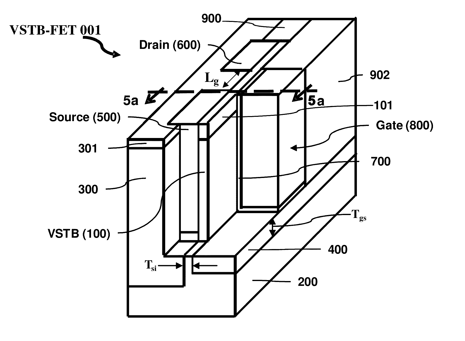
[0093]In an embodiment of the present invention, the VSTB-FET is a semiconductor on bulk c-Si transistor. The VSTB-FET is ideal for use in fully depleted VSTB transistor applications where the body electrical connection to the wafer substrate is essential, as illustrated in FIG. 4, FIG. 5a, and FIG. 5b.

[0094]The present invention is a semiconductor device comprising a semiconducting low doped vertical super-thin body (VSTB) connected to a vertical wall of a dielectric body, such as the STI, having the connecti...


PUM


Abstract

The present invention is a semiconductor device comprising a semiconducting low doped vertical super-thin body (VSTB) formed on Dielectric Body Wall (such as STI-wall as isolating substrate) having the body connection to bulk semiconductor wafer on the bottom side, isolation on the top side, and the channel, gate dielectric, and gate electrode on opposite to STI side surface. The body is made self-aligned to STI hard mask edge allowing tight control of body thickness. Source and Drain are made by etching holes vertically in STI at STI side of the body and filling with high doped crystalline or poly-Si appropriately doped with any appropriate silicides/metal contacts or with Schottky barrier Source/Drain. Gate first or Gate last approaches can be implemented. Many devices can be fabricated in single active area with body isolation between the devices by iso-plugs combined with gate electrode isolation by iso-trenches. The body can be made as an isolated nano-plate or set nano-wire MOSFET's on the STI wall to form VSTB SOI devices.

Description

CLAIM FOR PRIORITY[0001]The present invention claims priority to U.S. provisional patent application No. 61 / 713,003, filed on Nov. 8, 2012, by the inventor of the same name.INCORPORATION BY REFERENCE[0002]All publications mentioned herein are incorporated herein by reference to disclose and describe the methods and / or materials in connection with which the publications are cited. All publications, patents, and patent applications mentioned in this specification are herein incorporated by reference in their entirety and for all purposes to the same extent as if each individual publication, patent, or patent application was specifically and individually indicated to be incorporated by reference.[0003]Such incorporations include U.S. Pat. No. 8,120,073, inventors: Rakshit et al. entitled, “Trigate Transistor having Extended Metal gate Electrode”; U.S. Pat. No. 7,279,774, Inventors: Seo et al. entitled, “Bulk Substrates In FINFETS With Trench Insulation Surrounding Fin Pairs Having Fins...

Claims


Application Information

Patent Timeline
Patent Type & Authority Applications(United States)
IPC IPC(8): H01L21/8238
CPCH01L21/823814H01L27/1211H01L21/845H01L29/66795H01L29/785H01L2924/0002H10B12/36H10B12/056H10B10/12H10B41/30H01L2924/00H01L27/092H01L27/088H10B10/125H10B12/00H10B41/35H10B69/00H01L23/535H01L27/0886H01L29/0649H01L29/7851H01L23/528H01L27/1203H01L29/78603H01L29/78618H01L29/78696
Inventor KOLDIAEV, VIKTORPIROGOVA, RIMMA
Owner FINSCALE
Why Eureka
Try Eureka