Memory having three-dimensional structure and manufacturing method thereof

a three-dimensional structure and memory technology, applied in the field of memory, can solve the problems of short channel effect, punching, deficiency in the margin of a sensing current, etc., and achieve the effect of high integration and efficient enabling complicated contact functions

Inactive Publication Date: 2013-01-10
IUCF HYU (IND UNIV COOP FOUND HANYANG UNIV)
View PDF3 Cites 66 Cited by
  • Summary
  • Abstract
  • Description
  • Claims
  • Application Information

AI Technical Summary

Benefits of technology

[0022]According to the present invention, a step difference of a contact region connected to a word line is formed in a different direction from a direction in which the contact region extends from a cell region. That is, the step difference is formed in a second direction substantially perpendicular to a first direction in which the contact region extends. Also, a plurality of step difference groups are formed, thereby efficiently enabling complicated contact functions. As a result, a device can be highly integrated.
[0023]Furthermore, according to the present invention, an ONO layer and a conductive layer are formed on side surfaces of a multiple active layer that are exposed by removing a selective etching layer and preliminary etching layers. Thus, a cell transistor is embodied. Also, the conductive layer is formed of a metal material and controls operations of the cell transistor. One multilayered active layer includes a plurality of cell transistors, thereby enabling fabrication of a highly integrated nonvolatile memory device.

Problems solved by technology

In particular, a technique of improving the integration density of a flash memory by proportional reduction brings about a short channel effect, punch-through, and deficiency in the margin of a sensing current.

Method used


Image

  • Memory having three-dimensional structure and manufacturing method thereof
  • Memory having three-dimensional structure and manufacturing method thereof
  • Memory having three-dimensional structure and manufacturing method thereof

Examples


embodiment 1

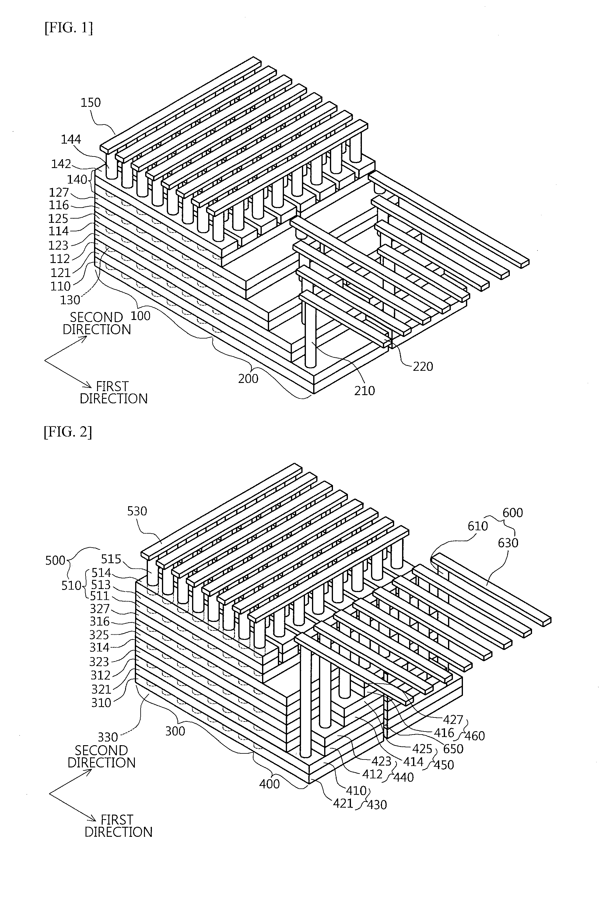
[0035]FIG. 2 is a perspective view of a flash memory according to a first exemplary embodiment of the present invention.

[0036]Referring to FIG. 2, the flash memory according to the present embodiment has a cell region 300, a contact region 400, a bit line interconnection region 500, and a word line interconnection region 600.

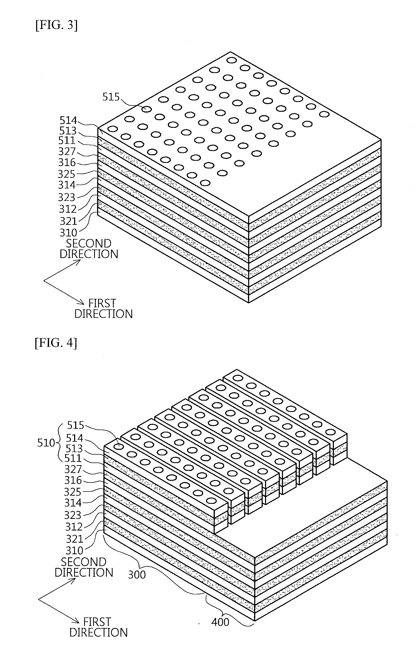
[0037]The cell region 100 includes cell transistors of the flash memory. To constitute the cell transistors, a plurality of insulating layers 310, 312, 314, and 316, a plurality of electrode layers 321, 323, 325, and 327, and plugs 330 formed through the insulating layers 310, 312, 314, and 316 and the electrode layers 321, 323, 325, and 327 are included.

[0038]The insulating layers 310, 312, 314, and 316 may be formed of any insulating material. Also, the electrode layers321, 323, 325, and 327 may be formed of any conductive material but are preferably formed of a metal material.

[0039]To begin with, the plurality of insulating layers 310, 312, 314, and 316 and t...

embodiment 2

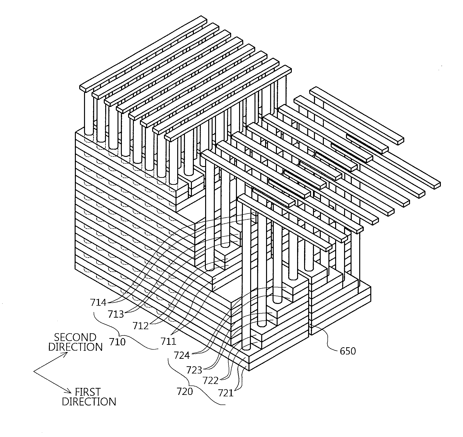
[0095]The flash memory obtained according to the above-described first embodiment may be fabricated using a structure in which a contact region has a double terminal.

[0096]FIG. 14 is a perspective view of a flash memory according to a second exemplary embodiment of the present invention.

[0097]Referring to FIG. 14, the flash memory is the same as shown in FIG. 2 except that step difference layers of a contact region 700 include two groups 710 and 720.

[0098]That is, the step difference layers include a first step difference group 710 and a second step difference group 720.

[0099]The second step difference group 720 is disposed at a lower end of the contact region 700 and protrudes in a first direction.

[0100]Also, the first step difference group 710 is disposed over the second step difference group 720 and closer to a cell region than the second step difference group 720. That is, the first step difference group 710 and the second step difference group 720 extend in the first direction ...

embodiment 3

[0112]FIGS. 20 through 33 are perspective views illustrating a method of fabricating a memory having a 3-dimensional structure according to a third exemplary embodiment of the present invention.

[0113]Referring to FIG. 20, preliminary etching layers 1310, 1312, 1314, and 1316 and insulating layers 1320, 1322, and 1324 are sequentially stacked on a substrate (not shown). A selective insulating layer 1326, a selective etching layer 1318, and a sacrificial layer 1328 are formed on the uppermost preliminary etching layer 1316. The insulating layers 1320, 1322, and 1324, the selective insulating layer 1326, and the sacrificial insulating layer 1328 are preferably formed of the same material. Also, a plurality of multilayered active layers 1330 are formed through the stacked insulating layers 1320, 1322, 1324, 1326, and 1328 and etching layers 1310, 1312, 1314, 1316, and 1318. The multilayered active layers 1330 are embodied by forming holes and filling the holes with poly-Si after forming...


PUM

PropertyMeasurementUnit
widthsaaaaaaaaaa
electrically connectedaaaaaaaaaa
areasaaaaaaaaaa

Abstract

Provided are a memory having a 3-dimensional structure and a method of fabricating the same, by which high integration density can be obtained. A contact region connected to a word line is formed to extend from a cell region in a first direction. A plurality of step difference layers constituting the contact region are formed to have step differences in a second direction different from the first direction. Also, provided is a method of fabricating a nonvolatile memory by which step differences are formed in a direction substantially perpendicular to a direction in which active regions are aligned. An insulating layer and etching layers are sequentially formed. By performing a selective etching process and pattern transfer, step differences are formed in a direction perpendicular to a direction in which multilayered active layers are disposed. Furthermore, the etching layers are removed using a wet etching process, and an oxide-nitride-oxide (ONO) layer and conductive layers are provided on the multilayered active layers having exposed side surfaces to form cell transistors. Thus, a memory having a high integration density is fabricated.

Description

TECHNICAL FIELD[0001]The present invention relates to a memory, and more particularly, to a memory having a 3-dimensional structure and a method of fabricating the same.BACKGROUND ART[0002]A flash memory, which is a typical nonvolatile memory device, operates based on a mechanism by which a state is changed by trapping and erasing charges. In recent years, a technique of improving integration density has been developed by conducting research into a device structure capable of proportionately reducing unit cells and embodying multi-bits.[0003]In particular, a technique of improving the integration density of a flash memory by proportional reduction brings about a short channel effect, punch-through, and deficiency in the margin of a sensing current. These phenomena naturally occur due to a reduction in the channel length of unit cells. To overcome these problems, a technique of 3-dimensionally embodying a structure of a flash memory has been developed.[0004]FIG. 1 is a perspective vi...

Claims


Application Information

Patent Timeline
Patent Type & Authority Applications(United States)
IPC IPC(8): H01L29/02H01L21/20H01L21/28
CPCH01L27/11582H01L27/11578H10B43/27H01L29/02
Inventor LEE, SEUNGBECKOH, SEULKILEE, JUNHYUK
Owner IUCF HYU (IND UNIV COOP FOUND HANYANG UNIV)
Why Eureka
Try Eureka