Probe card and method for manufacturing same

Active Publication Date: 2013-06-27
KOREA INST OF MASCH & MATERIALS
View PDF16 Cites 22 Cited by
  • Summary
  • Abstract
  • Description
  • Claims
  • Application Information

AI Technical Summary

Benefits of technology

[0031]According to an embodiment of the present invention, in the probe card, the number of contact probes may be efficiently increased without difficulty due to a manufacturing process, by increasing the number of unit plates instead of increasing the number of contact probes provided in one unit plate. Further, since the pitch of the el

Problems solved by technology

However, it is difficult to form a plurality of contact probes enough to test all semiconductor chips of a wafer by one process in one probe card, due to

Method used


Image

  • Probe card and method for manufacturing same
  • Probe card and method for manufacturing same
  • Probe card and method for manufacturing same

Examples


Embodiment Construction

[0039]The present invention will be described more fully hereinafter with reference to the accompanying drawings, in which exemplary embodiments of the invention are shown. As those skilled in the art would realize, the described embodiments may be modified in various different ways, all without departing from the spirit or scope of the present invention.

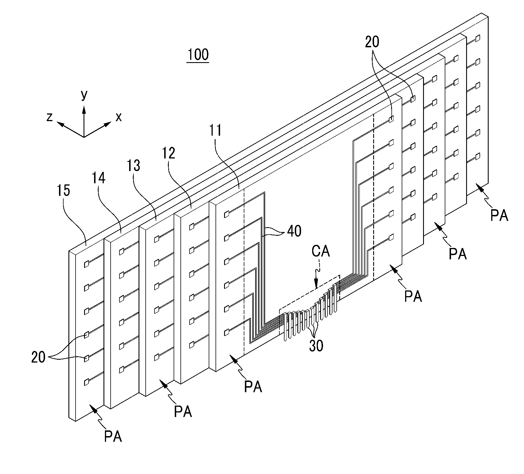
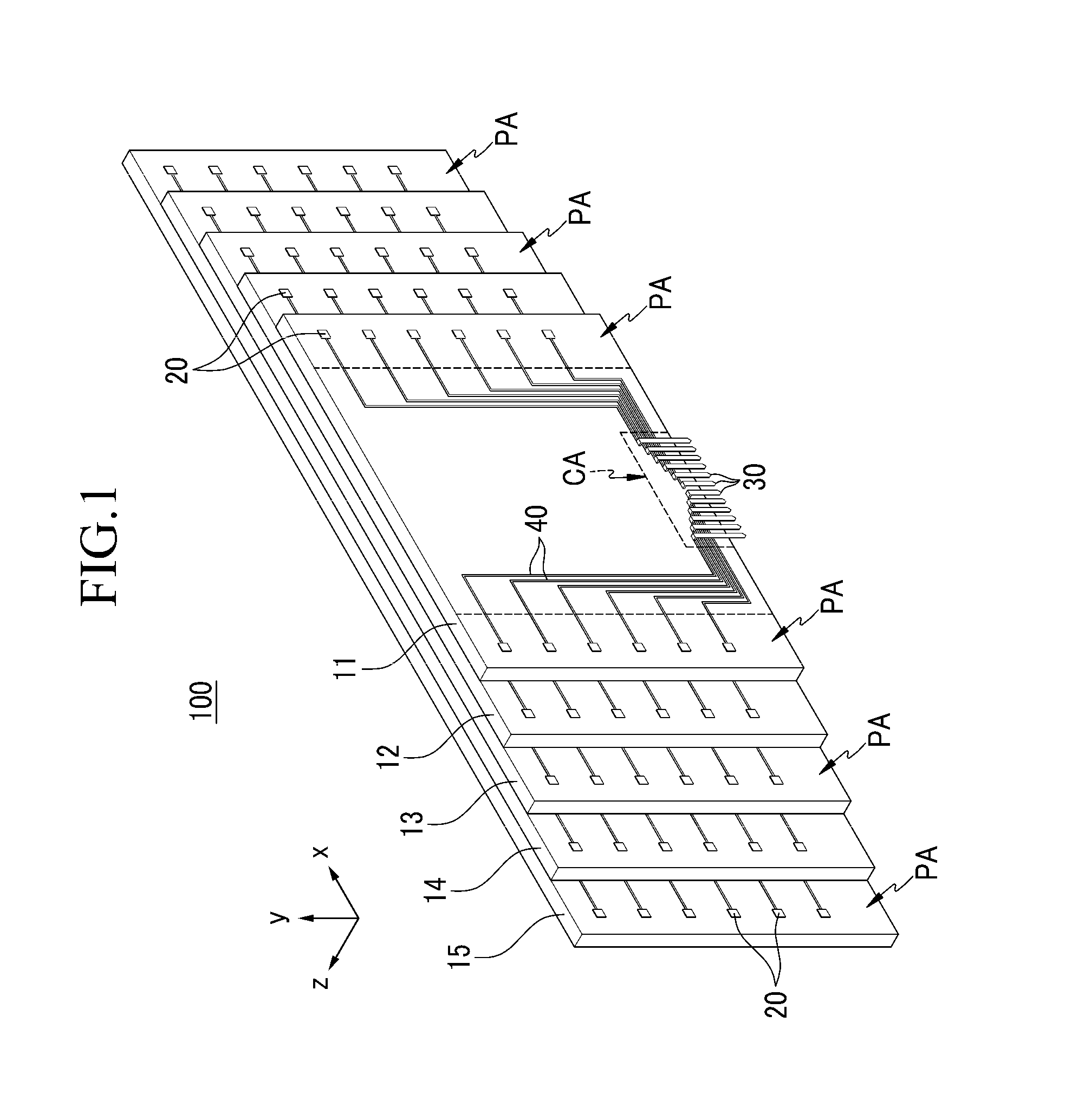
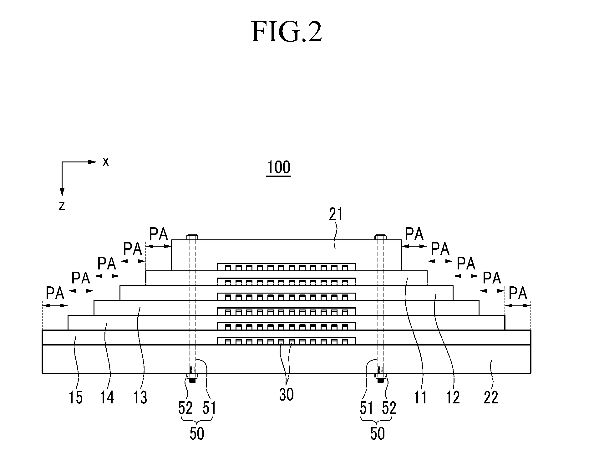
[0040]FIG. 1 is a perspective view illustrating a probe card according to a first exemplary embodiment of the present invention, and FIG. 2 is a bottom view of the probe card illustrated in FIG. 1.

[0041]Referring to FIGS. 1 and 2, a probe card 100 of the first exemplary embodiment has a structure in which a plurality of unit plates 11 to 15 having different sizes is laminated. In FIGS. 1 and 2, five unit plates are illustrated as an example, but the number of unit plates is not limited to the illustrated example and may be variously modified.

[0042]In each of the unit plates 11 to 15, a plurality of electrode pads 20, a plurality of ...


PUM

PropertyMeasurementUnit
Thicknessaaaaaaaaaa
Lengthaaaaaaaaaa
Thicknessaaaaaaaaaa

Abstract

Provided is a probe card including a plurality of unit plates including pad areas and contact probe areas, a plurality of electrode pads formed in the pad areas, a plurality of contact probes formed in the contact probe areas, and a plurality of interconnecting layers electrically connecting the electrode pads and the contact probes. The plurality of unit plates has different sizes and are arranged and laminated so as to expose all the pad areas of each unit plate.

Description

TECHNICAL FIELD[0001]The present invention relates to a probe card, and more particularly, to a probe card including an inspection circuit while high-densely arranging a plurality of contact probes for inspecting a highly integrated semiconductor chip, and a manufacturing method thereof.BACKGROUND ART[0002]Generally, a manufactured semiconductor chip performs an electrical inspection before packaging and after packaging, and good products are packaged and bad products are discarded according to the inspection result before packaging. A probe card which electrically connects a tester embedding a measuring device and an electrode pad of the semiconductor chip is used for the electrical inspection.[0003]A plurality of contact probes which is in contact with each electrode pad of the semiconductor chip to be electrically connected with the each electrode pad protrudes from the probe card. Each contact probe is connected with an electrode pad of the probe card through a interconnecting l...

Claims


Application Information

Patent Timeline
IPC IPC(8): G01R3/00G01R1/073
CPCG01R1/07307G01R3/00Y10T29/49126G01R1/07378G01R1/07342
Inventor LEE, HAK JOOKIM, JUNG YUPPARK, JUN-HYUB
Owner KOREA INST OF MASCH & MATERIALS
Why Eureka
Try Eureka