Semiconductor light emitting element and light emitting device

Active Publication Date: 2013-07-04
TOYODA GOSEI CO LTD
View PDF5 Cites 12 Cited by
  • Summary
  • Abstract
  • Description
  • Claims
  • Application Information

AI Technical Summary

Benefits of technology

The patent text explains how to make a semiconductor light emitting element produce light more efficiently, and keep it efficient even at high levels of current. This is achieved without changing the color of the light produced.

Problems solved by technology

Even such a semiconductor light emitting element that uses group-III nitride semiconductors and includes a light emitting layer having a multiquantum well structure suffers from reduction in the light emission efficiency in some cases when many holes or electrons are not recombined with each other in the multiple well layers of the light emitting layer.

Method used


Image

  • Semiconductor light emitting element and light emitting device
  • Semiconductor light emitting element and light emitting device
  • Semiconductor light emitting element and light emitting device

Examples


examples

[0128]Hereinafter, the present invention is described in more detail based on Examples. The present invention is not limited to the following examples within the scope of the present invention.

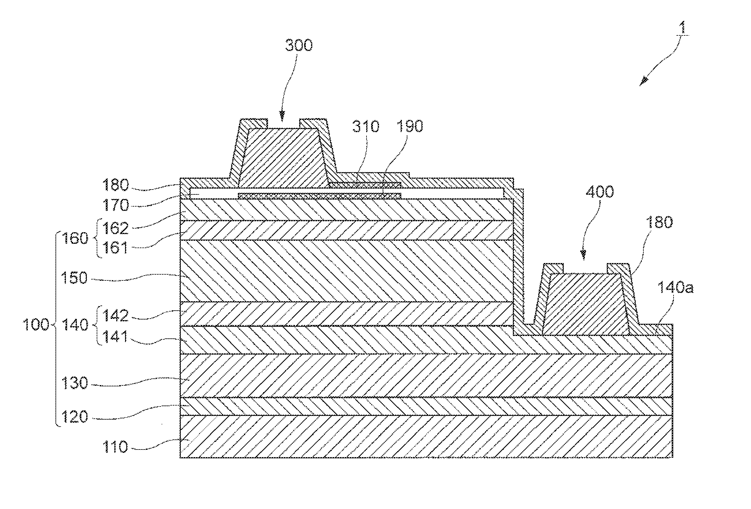
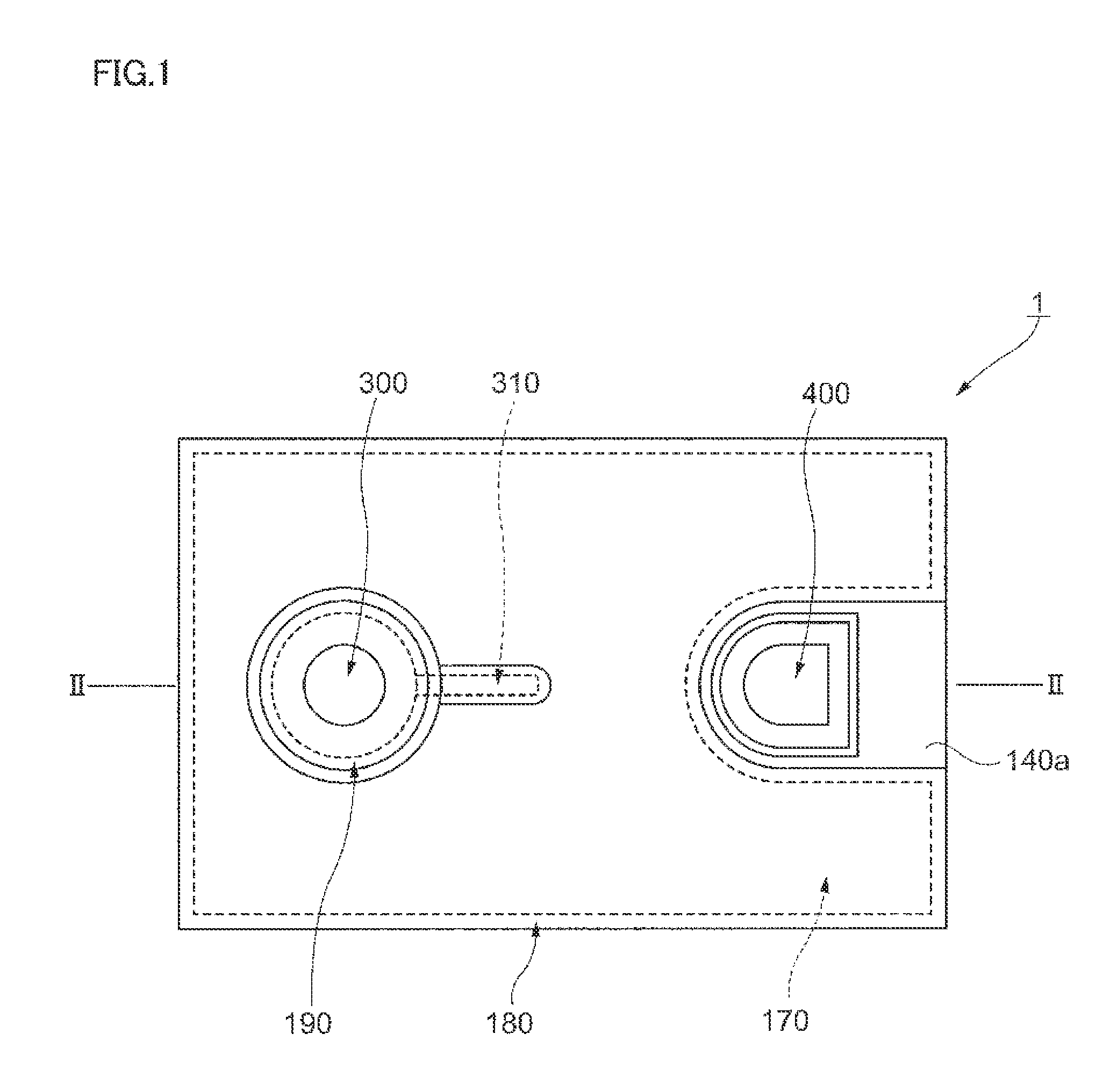
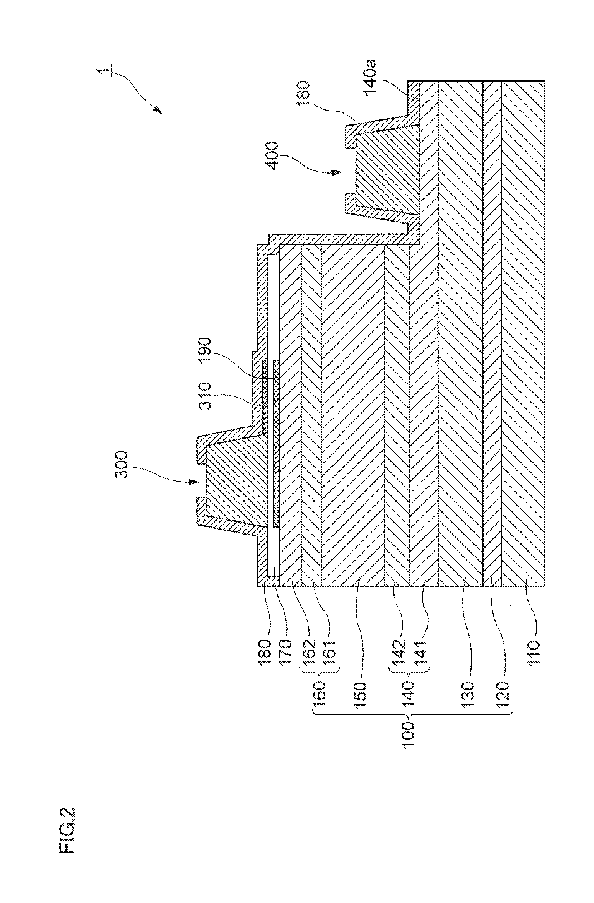
[0129]The inventor creates the semiconductor light emitting element 1 by varying the thickness and composition of the barrier layers 151 and well layers 152 of the light emitting layers 150 and performs various evaluations described below.

[0130]Herein, Table 1 shows configurations of Examples 1 to 10 of the semiconductor light emitting element 1, and Table 2 shows the configurations of Comparative Examples 1 to 7 of the semiconductor light emitting element 1. Tables 1 and 2 include, for each example, the thicknesses (nm) and compositions of the first to seventh barrier layers 1511 to 1517, which constitute the barrier layers 151, the thicknesses (nm) and compositions of the first to sixth well layers 1521 to 1526, which constitute the well layers 152, the total barrier thickness t10 (total thi...


PUM


Abstract

A semiconductor light emitting element includes an n-type semiconductor layer containing n-type impurities, a light emitting layer stacked on the n-type semiconductor layer, and a p-type semiconductor layer stacked on the light emitting layer and containing p-type impurities. The light emitting layer includes three or more well layers, and four or more barrier layers composed of a group-III nitride semiconductor having a larger band gap than that of the well layers, and each of the three or more well layers is sandwiched from both sides by neighboring two of the barrier layers. The three or more well layers include plural n-side well layers each having a first thickness to emit light of a common wavelength, and one or plural p-side well layers each having a second thickness larger than the first thickness and having a different composition from the n-side well layers to emit light of the common wavelength.

Description

CROSS REFERENCE TO RELATED APPLICATIONS[0001]This application is based on and claims priority under 35 USC §119 from Japanese Patent Application No. 2011-288601 filed Dec. 28, 2011.BACKGROUND[0002]1. Technical Field[0003]The present invention relates to a semiconductor light emitting element using group-III nitride semiconductors and a light emitting device provided with a semiconductor light emitting element.[0004]2. Related Art[0005]Generally, a semiconductor light emitting element using group-III nitride semiconductors includes a light emitting layer composed of a group-III nitride semiconductor between an n-type group-III nitride semiconductor layer and a p-type group-III nitride semiconductor layer. The n-type group-III nitride semiconductor layer contains n-type impurities for generating electrons as carriers, and the p-type group-III nitride semiconductor layer contains p-type impurities for generating holes as carriers. In this type of semiconductor light emitting elements, ...

Claims


Application Information

Patent Timeline
IPC IPC(8): H01L33/04
CPCH01L33/04H01L33/32H01L33/145H01L33/06
Inventor TERANISHI, SHUNSUKESATO, HISAO
Owner TOYODA GOSEI CO LTD
Why Eureka
Try Eureka