Electrode and Organic Electroluminescent Device Using Same
Active Publication Date: 2019-05-16
KUNSHAN NEW FLAT PANEL DISPLAY TECH CENT +1
View PDF1 Cites 2 Cited by
Summary
Abstract
Description
Claims
Application Information
AI Technical Summary
This helps you quickly interpret patents by identifying the three key elements:
Problems solved by technology
Method used
Benefits of technology
Benefits of technology
This patent provides a new electrode structure for organic light-emitting devices (OLEDs). The electrode consists of three layers: a first conductive layer, a second conductive layer, and a third conductive layer. The first and second layers have high transparency, while the third layer has low conductivity. This structure compensates for defects in the electrode and makes it more stable. The third layer has a low work function, which lowers the electron injection energy barrier and helps to increase the light-emitting efficiency of the device. Additionally, the second layer prevents the material of the first layer from dissolving in the material of the third layer, ensuring the stability of the electrode and improving the durability of the OLED. The electrode has good transparency and can be used as a transparent electrode.
Problems solved by technology
In order to increase the electron injection efficiency, the OLED cathode is supposed to use a metal material having its work function that should be as low as possible, and because electrons are more difficult to be injected than holes, the level of work function of the metal seriously affects the light-emitting efficiency and service life of an OLED device.
However, a single-layered metal cathode with a low work function, such as Mg, Ca, easily becomes oxidized in air, which causes the instability of device and shortens the service life of device, therefore, an alloy of metal with a low work function and anti-corrosion metal is usually selected to alleviate this problem.
When cathode film made of a single metal is evaporation-plated, a lot of defects would be formed, which leads to deterioration of the oxidative resistance thereof.
Method used
Image
Click on the blue label to locate the original text in one second.
Reading with bidirectional positioning of images and text.
Examples
embodiment 1
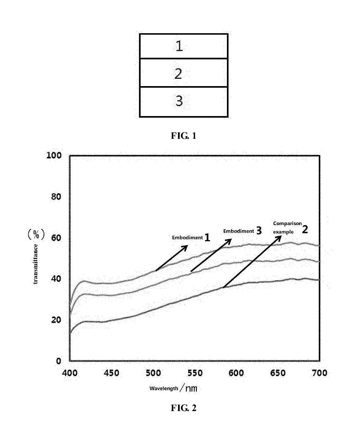
[0030]This embodiment provides an electrode, as shown in FIG. 1, the electrode comprises a first conductive layer 1 and a second conductive layer 2 that are arranged in a stacked manner. The first conductive layer 1 is Ag layer with a thickness of 16 nm, the second conductive layer 2 is Mg layer with a thickness of lnm, and a third conductive layer 3 is Yb layer with a thickness of 1 nm.
[0035]The layer of CBP (N′-di-carbazolyl-biphenyl) doped with Ir(piq)3 (Tri-(1-phenylisoquinolinato-C2,N]-Iridium(III)) is a light...
embodiment 2
[0040]This embodiment provides an electrode with a structure similar to that of Embodiment 1, but the difference is that the third conductive layer is Yb2O3 layer with a thickness of lnm.
[0041]This embodiment also provides an organic electroluminescent device with a structure similar to that of Embodiment 1, but the difference is that the second electrode is the electrode according to this embodiment:
[0043]This embodiment provides an electrode with a structure similar to that of Embodiment 1, but the difference is that the second conductive layer is an alloy layer of Mg and Ag with a thickness of 2 nm, and the first conductive layer has a thickness of 5 nm.
[0044]This embodiment also provides an organic electroluminescent device with a structure similar to that of Embodiment 1, but the difference is that the second electrode is the electrode according to this embodiment.
PUM
Abstract
An electrode and an organic electroluminescent device using the same are provided. The electrode comprises a first conductive layer (1), a second conductive layer (2) and a third conductive layer (3) that are arranged in a stacked manner The second conductive layer (2) has a single-layer structure or multi-layer composite structure formed by at least one of alkali earth metal, alkali earth metalalloy and alkali earth metal compound, and the third layer (3) has a work function of less than 3 eV. The respective conductive layers of the electrode can compensate with respect to the defects in one another, thereby making the performance of the electrode more stable. In the meantime, because the work function of the third conductive layer (3) is less than 3 eV, the barrier of organics-metal interface can be effectively reduced for guiding the electron injection, thereby increasing the light-emitting efficiency of device. Also, because the electrode has relatively good transmittance, it can be used as a transparent electrode.
Description
TECHNICAL FIELD[0001]The present disclosure relates to the field of organic electroluminescence, and particularly relates to an electrode and an organic electroluminescent device using the same.BACKGROUND[0002]An organic light-emitting diode (OLED) is an active light-emitting device. As compared to thin-film-transistorliquid crystal display (LCD) and plasma display panel (PDP) in the prior art of panel display technologies, an organic light-emitting display device using organic light-emitting diodes has advantages such as high contrast ratio, wide viewing angle, low power consumption and thinner volume, is expected to become the next-generation mainstream panel display technology, and is one of the panel display technologies that has received the most attention at present.[0003]An OLED device mainly comprises an anode, an organic light-emitting layer and a cathode that are arranged in a stacked manner. In order to increase the electron injection efficiency, the OLEDcathode is supp...
Claims
Application Information
Patent Timeline
Application Date:The date an application was filed.
Publication Date:The date a patent or application was officially published.
First Publication Date:The earliest publication date of a patent with the same application number.
Issue Date:Publication date of the patent grant document.
PCT Entry Date:The Entry date of PCT National Phase.
Estimated Expiry Date:The statutory expiry date of a patent right according to the Patent Law, and it is the longest term of protection that the patent right can achieve without the termination of the patent right due to other reasons(Term extension factor has been taken into account ).
Invalid Date:Actual expiry date is based on effective date or publication date of legal transaction data of invalid patent.

