Highly Flexible Near-infrared Metamaterials

a nano-material, near-infrared technology, applied in the direction of instruments, synthetic resin layered products, transportation and packaging, etc., can solve the problems of additional difficulty in focusing electrons in ebl process on the surface of pet substrates, limited optical functionality of such kinds of nano-structures,

Active Publication Date: 2013-07-11
HONG KONG BAPTIST UNIV
View PDF0 Cites 15 Cited by
  • Summary
  • Abstract
  • Description
  • Claims
  • Application Information

AI Technical Summary

Benefits of technology

[0006]Embodiments of the present invention include a novel multilayer flexible metamaterial that can work at near infrared (NIR) regime that can be fabricated on transparent PET substrate using flip chip transfer (FCT) technique. An embodiment of the present invention also provides novel NIR metamaterial device that can be transformed into various shapes by bending the PET substrate, wherein said metamaterial device is tunable via physical manipulation of its flexible substrate with no requirement to change the material composition of the substrate. The flexibility allows the novel NIR metamaterial device to bend and stretch, which can alter the device structure. Since the resonant frequency of each device is a function of the device structure, the resonant frequency can be tuned by the bend and stretch of the substrate. Another embodiment of the present invention is the fabrication method, which allows the transfer of the metamaterial from a rigid substrate such as glass, quartz and metals onto a flexible substrate such as plastic or polymer film. Thus, a flexible metamaterial can be fabricated independent of the original substrate used. Another embodiment of the present invention further provides novel tunable sensors and emitters using such flexible metamaterials and devices.

Problems solved by technology

Optical functionality of such kinds of nanostructures is limited by the planar surface and thus sensitive to the incident angle of light.
Besides, the curved surface of the PET substrate brings additional difficulty for the focusing of electron in EBL process.

Method used


Image

  • Highly Flexible Near-infrared Metamaterials
  • Highly Flexible Near-infrared Metamaterials
  • Highly Flexible Near-infrared Metamaterials

Examples


Embodiment Construction

[0024]The present invention is not to be limited in scope by any of the specific embodiments described herein. The following embodiments are presented for exemplification only.

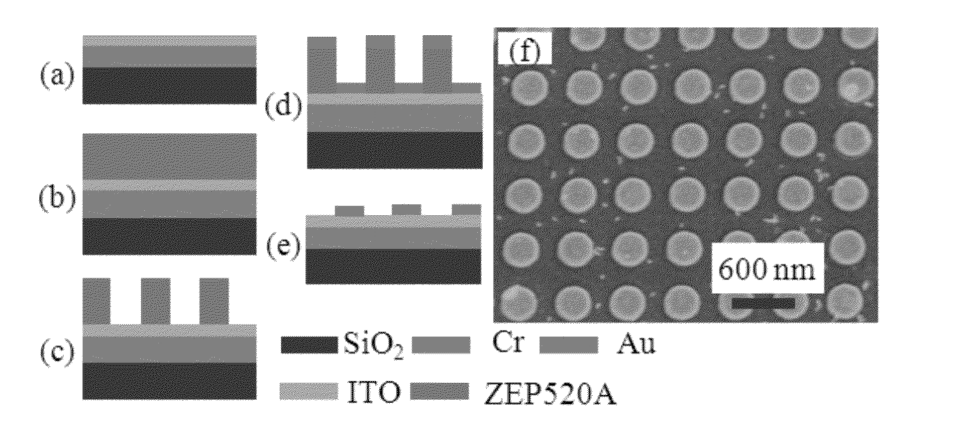
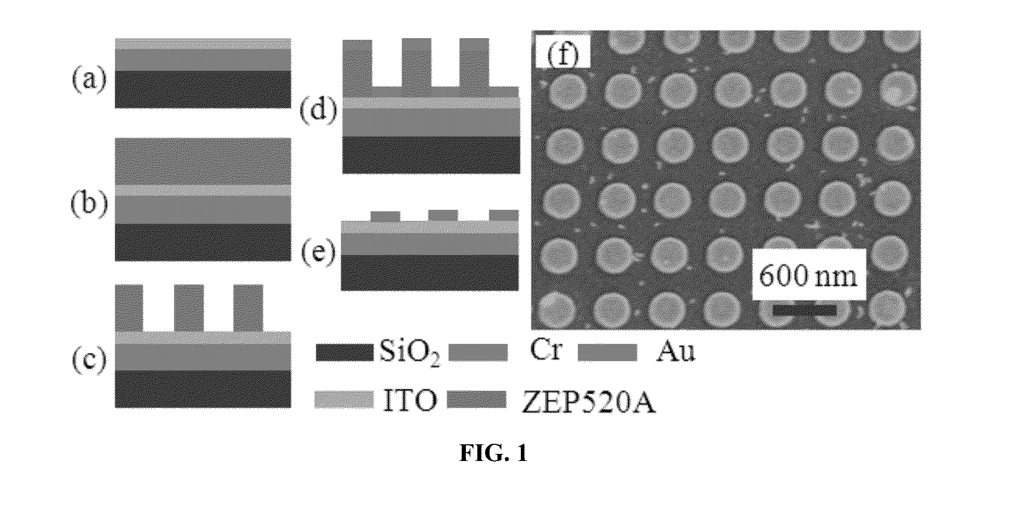
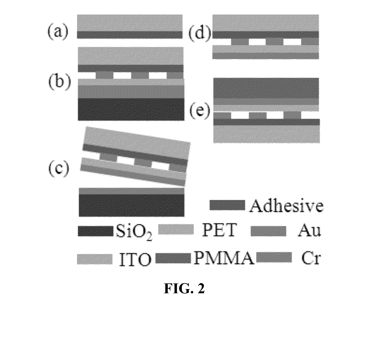
[0025]The present invention provides a novel multilayer flexible metamaterial can be fabricated using flip chip transfer (FCT) technique. This technique is different from other similar techniques such as metal lift off process, which fabricates the nanostructures directly onto the flexible substrate or nanometer printing technique. It is a solution-free FCT technique using double-side optical adhesive as the intermediate transfer layer and a tri-layer metamaterial nanostructures on a rigid substrate, which can be transferred onto the adhesive first. Another embodiment of the present invention is the fabrication method, which allows the transfer of the novel metamaterial from a rigid substrate such as glass, quartz and metals onto a flexible substrate such as plastic or polymer film. Thus, a novel flexible meta...


PUM

PropertyMeasurementUnit
thicknessaaaaaaaaaa
thicknessaaaaaaaaaa
diameteraaaaaaaaaa

Abstract

A novel multilayer flexible metamaterial that can work at near infrared (NIR) regime that can be fabricated on transparent PET substrate using flip chip transfer (FCT) technique. An embodiment of the present invention also provides novel NIR metamaterial device that can be transformed into various shapes by bending the PET substrate, wherein said metamaterial device is tunable via physical manipulation of its flexible substrate with no requirement to change the material composition of the substrate. The flexibility allows the novel NIR metamaterial device to bend and stretch, which can alter the device structure. Since the resonant frequency of each device is a function of the device structure, the resonant frequency can be tuned by the bend and stretch of the substrate. Another embodiment of the present invention further provides novel tunable sensors and emitters using such flexible metamaterials and devices.

Description

CROSS-REFERENCE TO RELATED APPLICATIONS[0001]The present application claims priority to the U.S. Provisional Patent Application No. 61 / 579,668 filed Dec. 23, 2011; the disclosure of which is incorporated herein by reference in its entirety.FIELD OF INVENTION[0002]The present invention relates to a novel plasmonic or metamaterial nanostructures. In particular, the present invention relates to a novel tri-layer flexible metamaterials that can work at near infrared (NIR) regime that can be fabricated on transparent polyethylene terephthalate (PET) substrate using flip chip transfer (FCT) technique. FCT technique is solution-free and can also be applied to fabricate other functional nanostructures device on flexible substrate. This invention also provides novel NIR metamaterial device that can be transformed into various shapes by bending the PET substrate. This invention further provides novel tunable sensors and emitters using such flexible metamaterials and devices.BACKGROUND OF INVE...

Claims


Application Information

Patent Timeline
Patent Type & Authority Applications(United States)
IPC IPC(8): B32B27/36
CPCB32B27/36G02F2202/30G02B1/002G02F1/01Y10T428/31786B32B3/30B32B7/06B32B7/12B32B38/10B32B37/26B32B37/12B32B37/144B32B3/16
Inventor CHEAH, KOK WAILI, GUIXIN
Owner HONG KONG BAPTIST UNIV
Why Eureka
Try Eureka