Power semiconductor module and method of manufacturing the same

a technology of power semiconductor modules and manufacturing methods, applied in semiconductor devices, semiconductor/solid-state device details, electrical apparatus, etc., can solve the problems of limited thermal resistance measurement, complicated manufacturing, and increased cost, and achieve the effect of reducing the cost of a power semiconductor module and high cooling performan

Active Publication Date: 2013-07-18
MITSUBISHI ELECTRIC CORP
View PDF8 Cites 35 Cited by
  • Summary
  • Abstract
  • Description
  • Claims
  • Application Information

AI Technical Summary

Benefits of technology

[0010]An object of the present invention is to provide the technology for ...

Problems solved by technology

In view of an increase in capacity of a module as descried above, however, such a measure against thermal resistance is limited.
This configuration requires a plurality of spacers and a plurality of heat dissipating plates in a case of a semiconductor module containing a plurality of s...

Method used


Image

  • Power semiconductor module and method of manufacturing the same
  • Power semiconductor module and method of manufacturing the same
  • Power semiconductor module and method of manufacturing the same

Examples


first preferred embodiment

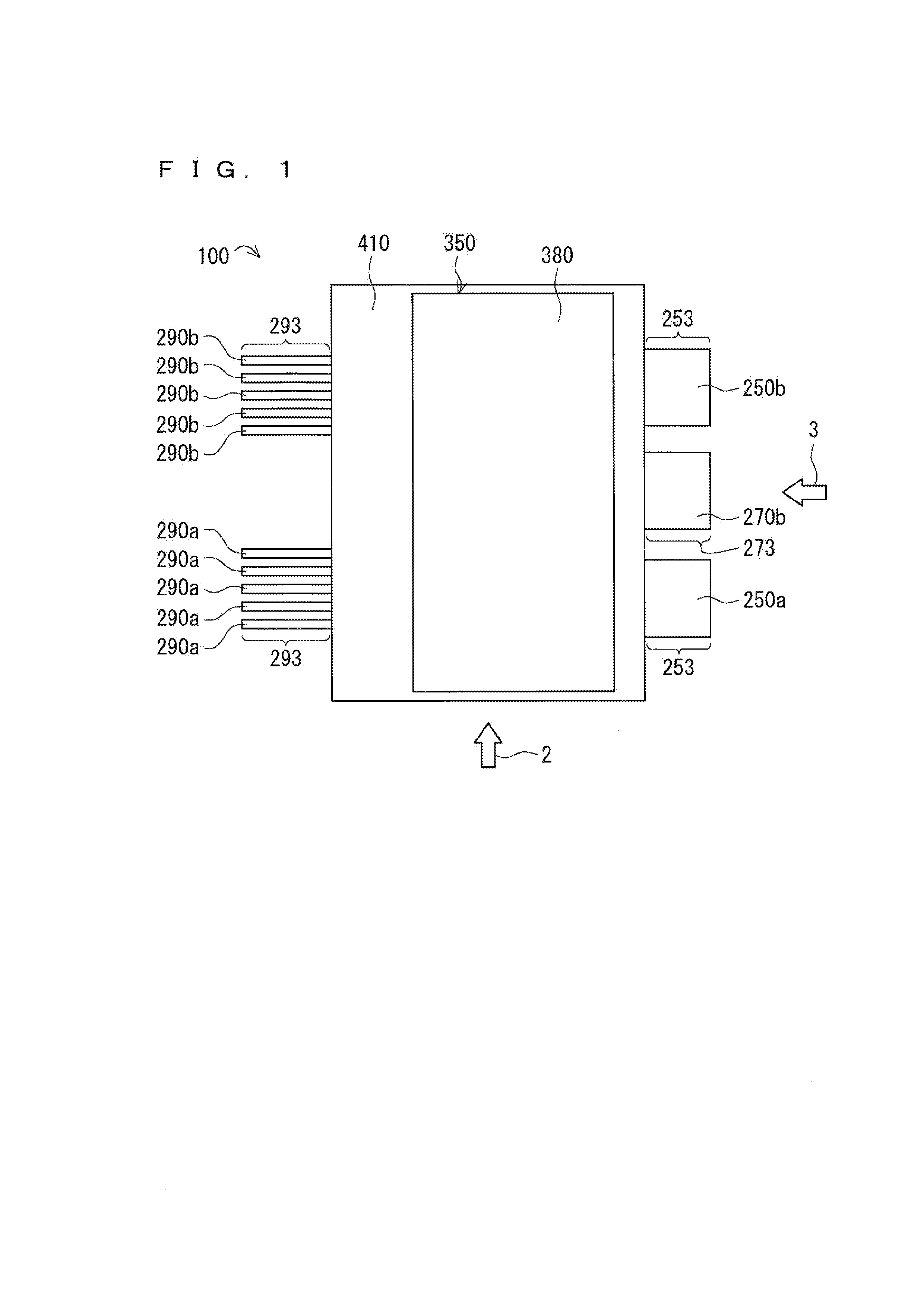
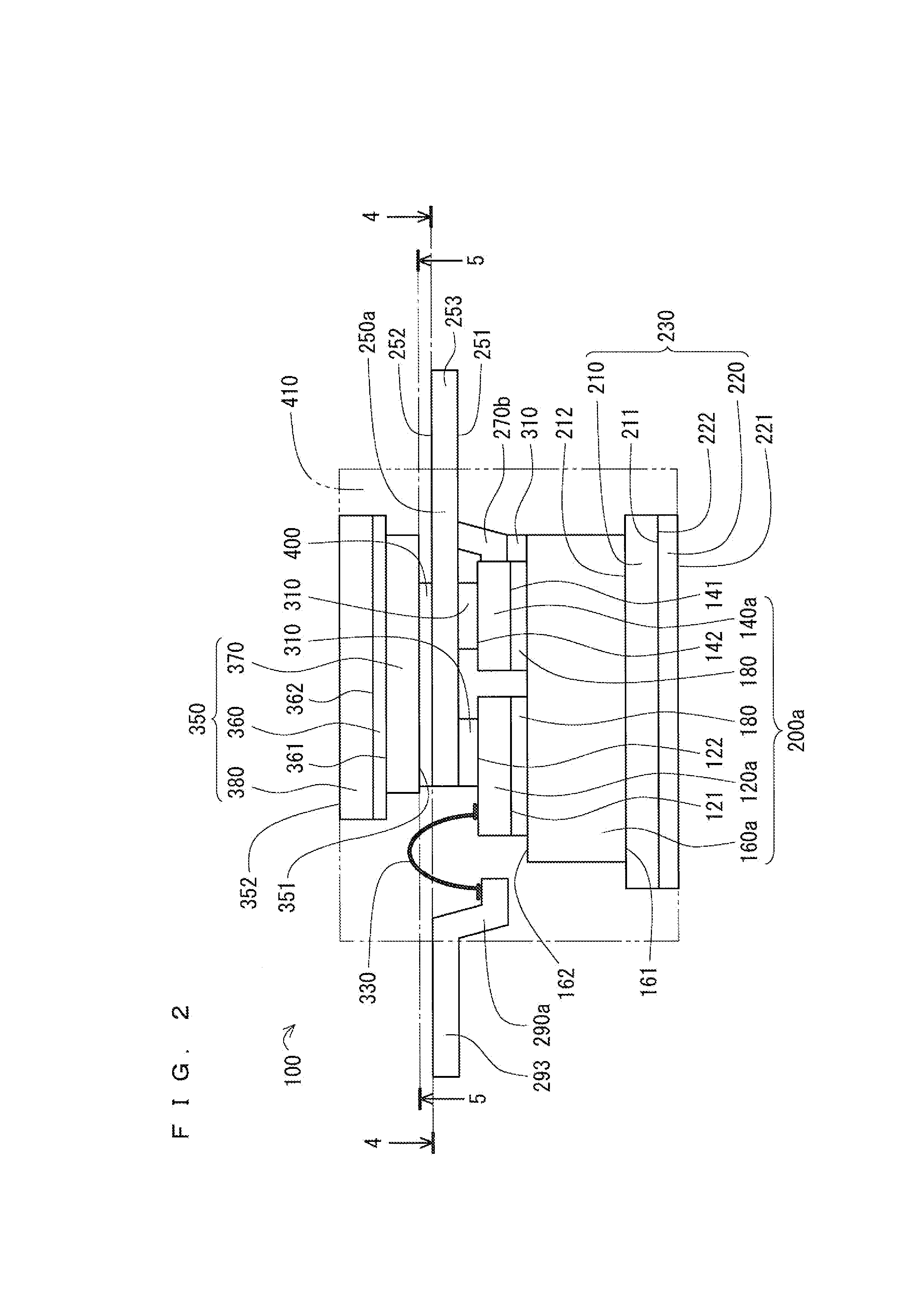
[0042]FIGS. 1 to 5 show the configuration of a power semiconductor module 100 according to a first preferred embodiment. Specifically, FIG. 1 is a plan view (top view) of the power semiconductor module 100. FIG. 2 is a side view of the power semiconductor module 100 when viewed from a direction of an arrow 2 in FIG. 1, and FIG. 3 is a side view of the power semiconductor module 100 when viewed from a direction of an arrow 3 in FIG. 1. FIG. 4 is a plan view of the power semiconductor module 100 when viewed from an arrow at a position indicated by a line 4-4 in FIGS. 2 and 3. FIG. 5 is a plan view of the power semiconductor module 100 when viewed from an arrow at a position indicated by a line 5-5 in FIGS. 2 and 3. Note that FIGS. 2 to 5 show the state in which a molding resin described below (see reference numeral 410; an external shape thereof is indicated by a chain double-dashed line for reference) is removed for the sake of description. FIG. 6 is a circuit diagram of the power se...

second preferred embodiment

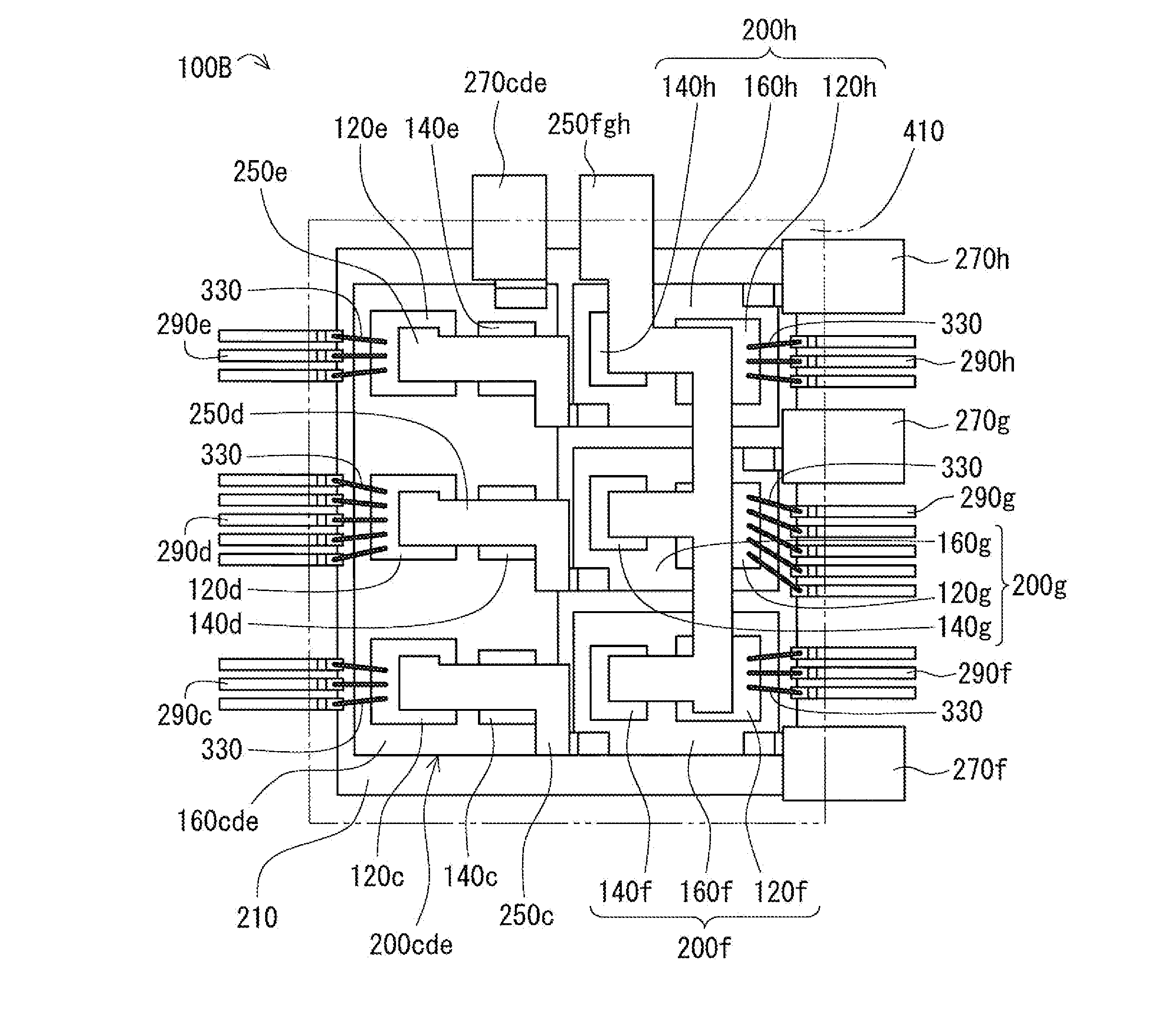
[0117]FIGS. 9 to 12 are views showing the configuration of a power semiconductor module 100B according to a second preferred embodiment. Specifically, FIG. 9 is a plan view (top view) of the power semiconductor module 100B. FIG. 10 is a side view of the power semiconductor module 100B when viewed from a direction of an arrow 10 in FIG. 9. FIG. 11 is a plan view of the power semiconductor module 100B when viewed from a direction of an arrow at the position indicated by a line 11-11 in FIG. 10. FIG. 12 is a plan view of the power semiconductor module 100B when viewed from a direction of an arrow at the position indicated by a line 12-12 in FIG. 10. FIGS. 10 to 12 show the state in which the molding resin 410 (an external shape thereof is indicated by a chain double-dashed line for reference) is removed for the sake of description. FIG. 13 is a circuit diagram of the power semiconductor module 100B.

[0118]According to the example of FIGS. 9 to 12, the power semiconductor module 100B inc...

third preferred embodiment

[0178]FIGS. 16 to 19 are views showing the configuration of a power semiconductor module 100C according to a third preferred embodiment. Specifically, FIG. 16 is a plan view (top view) of the power semiconductor module 100C. FIG. 17 is a side view of the power semiconductor module 100C when viewed from a direction of an arrow 17 in FIG. 16. FIG. 18 is a plan view of the power semiconductor module 100C when viewed from a direction of an arrow at the position indicated by a line 18-18 in FIG. 17. FIG. 19 is a plan view of the power semiconductor module 100C when viewed from a direction of an arrow at the position indicated by a line 19-19 in FIG. 17. FIGS. 17 to 19 show the state in which the molding resin 410 (an external shape thereof is indicated by a chain double-dashed line for reference) is removed for the sake of description. FIG. 20 is a circuit diagram of the power semiconductor module 100C.

[0179]According to the example of FIGS. 16 to 19, the power semiconductor module 100C ...


PUM


Abstract

First chip main surfaces of first semiconductor chips are bonded to a heat spreader, and second chip main surfaces of the first semiconductor chips are bonded to a first electrode. First chip main surfaces of second semiconductor chips are bonded to a heat spreader, and second chip main surfaces of the second semiconductor chips are bonded to a first electrode. A plurality of electrodes are provided by a lead frame. An insulating member is provided on a side opposite to the chips when viewed from the heat spreader. An insulating substrate is provided on a side opposite to the chips when viewed from the first electrodes.

Description

BACKGROUND OF THE INVENTION[0001]1. Field of the Invention[0002]The present invention relates to a power semiconductor module of resin-sealed type and a method of manufacturing the same.[0003]2. Description of the Background Art[0004]Recently, advances have been made which allow power semiconductor modules to, for example, have a larger capacity, a more compact size and a higher frequency. The heat generation density of a semiconductor element becomes higher along with this, which requires high cooling performance.[0005]In a conventional cooling structure, a cooler is mounted onto one outer surface of a power semiconductor module, and the heat generated by the semiconductor element inside the module is transferred to the cooler and is dissipated. In this case, it is possible to improve cooling performance by reducing a thermal resistance of a member constituting a heat transfer path ranging from the semiconductor element to the cooler. In view of an increase in capacity of a module ...

Claims


Application Information

Patent Timeline
IPC IPC(8): H01L25/07H01L21/98H01L29/161
CPCH01L2924/13091H01L2224/48091H01L2224/48247H01L2224/49175H01L2224/73265H01L23/4334H01L23/49541H01L23/49575H01L2924/13055H01L2224/40139H01L23/3107H01L24/33H01L24/40H01L24/73H01L2224/32245H01L2224/33181H01L2224/45124H01L2224/73215H01L2224/40247H01L2224/73213H01L2924/10253H01L21/561H01L24/29H01L24/32H01L24/37H01L24/45H01L24/48H01L24/49H01L24/92H01L24/97H01L2224/06181H01L2224/291H01L2224/92246H01L2224/92247H01L2224/97H01L2924/10272H01L2924/1203H01L2224/3755H01L2224/73221H01L2924/014H01L2924/1306H01L2924/1305H01L2924/00014H01L2924/00H01L2924/00012H01L2224/85H01L2224/83H01L2224/84H01L2924/351H01L2224/40137H01L2924/181H01L2224/84801H01L2224/83801H01L24/84H01L2224/0603
Inventor USUI, OSAMUYOSHIMATSU, NAOKIKIKUCHI, MASAO
Owner MITSUBISHI ELECTRIC CORP
Why Eureka
Try Eureka