Bumping process and structure thereof

a technology of a copper bump and a structure, applied in the direction of semiconductor devices, semiconductor/solid-state device details, electrical devices, etc., to achieve the effect of increasing the density of the circuit layout and reducing the distance between two adjacent copper bumps

Inactive Publication Date: 2013-08-01
CHIPBOND TECH
View PDF2 Cites 13 Cited by
  • Summary
  • Abstract
  • Description
  • Claims
  • Application Information

AI Technical Summary

Benefits of technology

[0003]The primary object of the present invention is to provide a bumping process comprising the steps of providing a silicon substrate having a surface, a plurality of bond pads disposed on said surface, and a protective layer disposed on said surface, wherein the protective layer comprises a plurality of openings, and the bond pads are revealed by the openings; forming a titanium-containing metal layer on the silicon substrate, said titanium-containing metal layer covers the protective layer and the bond pads and comprises a plurality of first areas and a plurality of second areas located outside the first areas; forming a first photoresist layer on the titanium-containing metal layer; patterning the first photoresist layer to form a plurality of first opening slots, wherein each of the first opening slots is corresponded to each of the first areas of the titanium-containing metal layer; forming a plurality of copper bumps within the first opening slots, each of the copper bumps comprises a first top surface and a first ring surface; removing the first photoresist layer to reveal the first top surfaces of the copper bumps, the first ring surfaces, and the second areas of the titanium-containing metal layer; forming a second photoresist layer on the titanium-containing metal layer and covering the copper bumps with the second photoresist layer; patterning the second photoresist layer to form a plurality of second opening slots, wherein each of the second opening slots is corresponded to each of the copper bumps and comprises an inner lateral surface, and a space located between the inner lateral surface of each of the second opening slots and the first ring surface of each of the copper bumps; forming a plurality of bump isolation layers at the spaces, the first top surfaces and the first ring surfaces, and each of the bump isolation layers comprises a second top surface; forming a plurality of connective layers on the second top surfaces of the bump isolation layers; removing the second photoresist layer; removing the second areas of the titanium-containing metal layer and enabling each of the first areas of the titanium-containing metal layer to form an under bump metallurgy layer located beneath the copper bump. Owning to the reason that each of the bump isolation layers covers the first ring surface and the first top surface of each of the copper bumps, a short phenomenon occurred between two adjacent copper bumps via dissociation of copper ions can be prevented. Therefore, the distance between two adjacent copper bumps can be reduced so as to increase the circuit layout density.

Problems solved by technology

However, a short distance between two adjacent electronic connection devices makes a short phenomenon easily occurred in circuit layout.

Method used


Image

  • Bumping process and structure thereof
  • Bumping process and structure thereof
  • Bumping process and structure thereof

Examples


Embodiment Construction

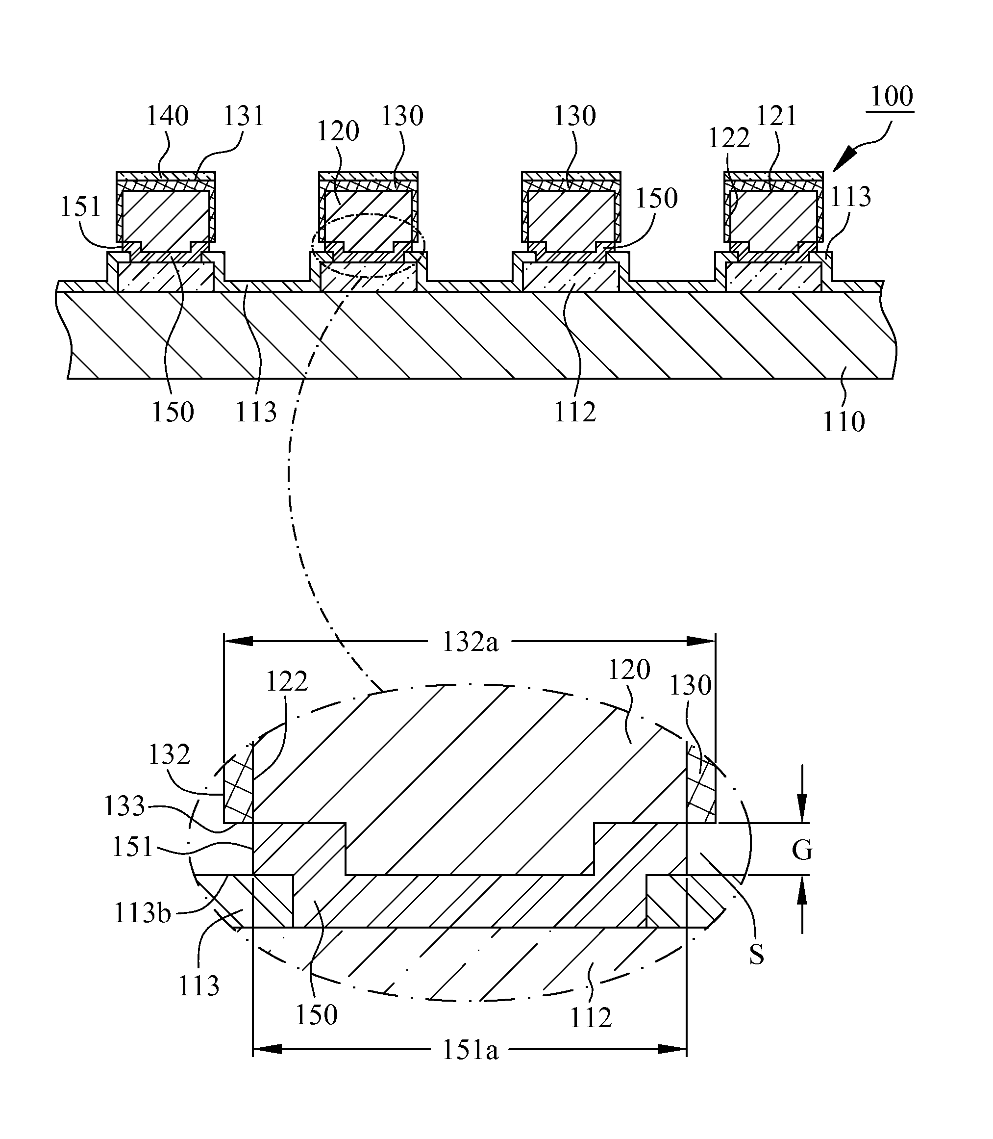
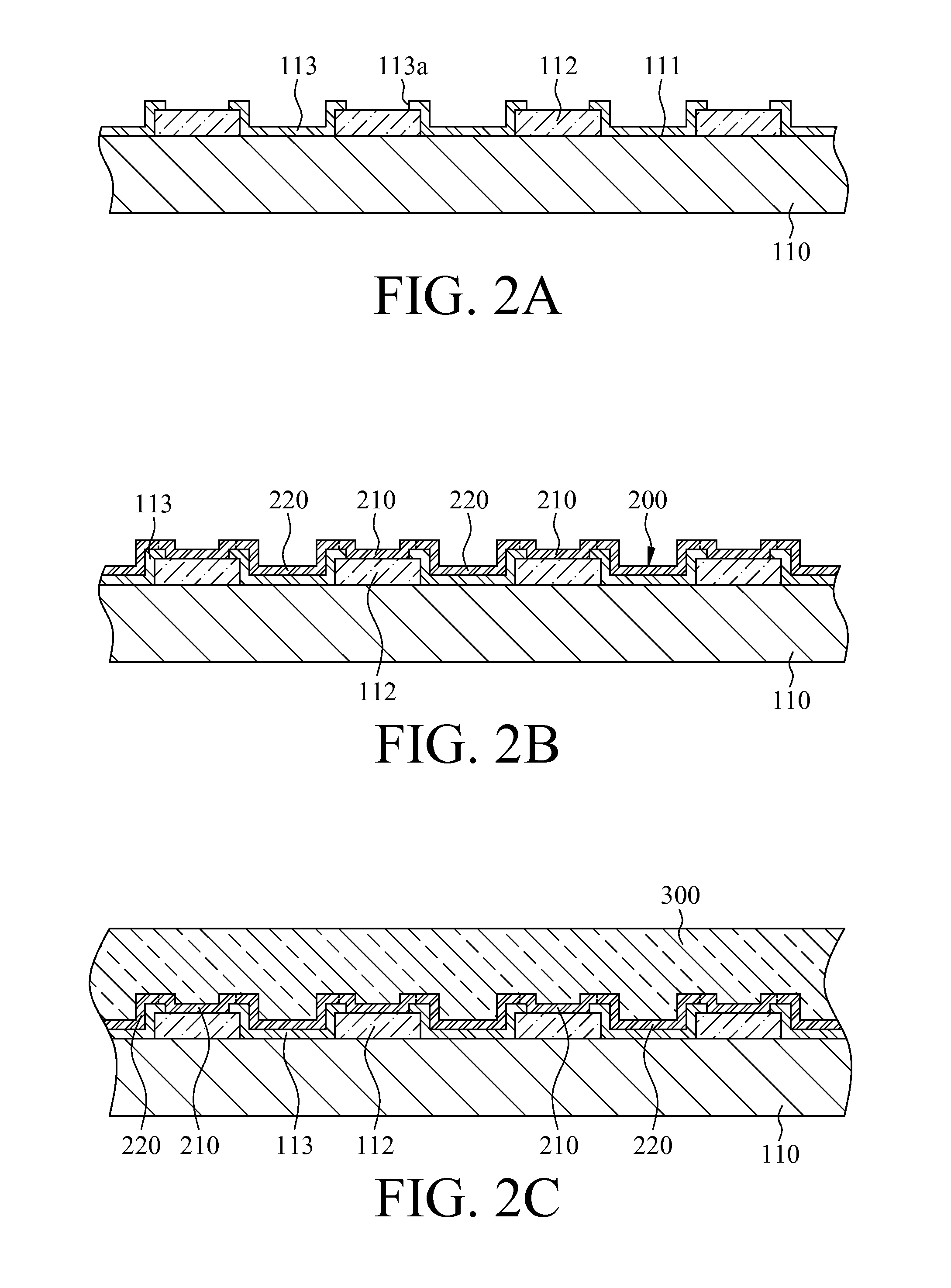
[0006]With reference to FIGS. 1 and 2A-2L, a bumping process in accordance with a preferred embodiment of the present invention comprises the steps described as followed. First, referring to step 10 of FIG. 1 and FIG. 2A, providing a silicon substrate 110 having a surface 111, a plurality of bond pads 112 disposed on said surface 111, and a protective layer 113 disposed on said surface 111, wherein the protective layer 113 comprises a plurality of openings 113a, and the bond pads 112 are revealed by the openings 113a. Next, with reference to step 11 of FIG. 1 and FIG. 2B, forming a titanium-containing metal layer 200 on the silicon substrate 110, said titanium-containing metal layer 200 covers the protective layer 113 and the bond pads 112, and said titanium-containing metal layer 200 comprises a plurality of first areas 210 and a plurality of second areas 220 located outside the first areas 210. Thereafter, referring to step 12 of FIG. 1 and FIG. 2C, forming a first photoresist lay...


PUM

PropertyMeasurementUnit
areasaaaaaaaaaa
circumferenceaaaaaaaaaa
outer circumferenceaaaaaaaaaa

Abstract

A bumping process includes providing a silicon substrate; forming a titanium-containing metal layer on silicon substrate, the titanium-containing metal layer comprises a plurality of first areas and a plurality of second areas; forming a first photoresist layer on titanium-containing metal layer; patterning the first photoresist layer to form a plurality of first opening slots; forming a plurality of copper bumps within first opening slots, said copper bump comprises a first top surface and a first ring surface; removing the first photoresist layer; forming a second photoresist layer on titanium-containing metal layer; patterning the second photoresist layer to form a plurality of second opening slots; forming a plurality of bump isolation layers at spaces, the first top surfaces and the first ring surfaces; forming a plurality of connective layers on bump isolation layers; removing the second photoresist layer, removing the second areas to form an under bump metallurgy layer.

Description

FIELD OF THE INVENTION[0001]The present invention is generally related to a bumping process and structure thereof, which particularly relates to the bumping process which improves manufacturing yield.BACKGROUND OF THE INVENTION[0002]Modern electronic products gradually lead a direction of light, thin, short, and small. Accordingly, the layout density of interior circuit for electronic product becomes more concentrated consequentially. However, a short distance between two adjacent electronic connection devices makes a short phenomenon easily occurred in circuit layout.SUMMARY[0003]The primary object of the present invention is to provide a bumping process comprising the steps of providing a silicon substrate having a surface, a plurality of bond pads disposed on said surface, and a protective layer disposed on said surface, wherein the protective layer comprises a plurality of openings, and the bond pads are revealed by the openings; forming a titanium-containing metal layer on the ...

Claims


Application Information

Patent Timeline
Patent Type & Authority Applications(United States)
IPC IPC(8): H01L23/498H01L21/768
CPCH01L24/11H01L2224/0401H01L2224/05027H01L24/03H01L24/05H01L24/13H01L2224/034H01L2224/05184H01L2224/05644H01L2224/05647H01L2224/11903H01L2224/13147H01L2224/13562H01L2224/13564H01L2224/13582H01L2224/13644H01L2224/13655H01L2224/13664H01L2224/03912H01L2224/11472H01L2224/05572H01L21/76885H01L2924/00014H01L2224/05552
Inventor KUO, CHIH-MINGCHIU, YIE-CHUANHO, LUNG-HUA
Owner CHIPBOND TECH
Why Eureka
Try Eureka