Solid-state imaging device and method for manufacturing the same

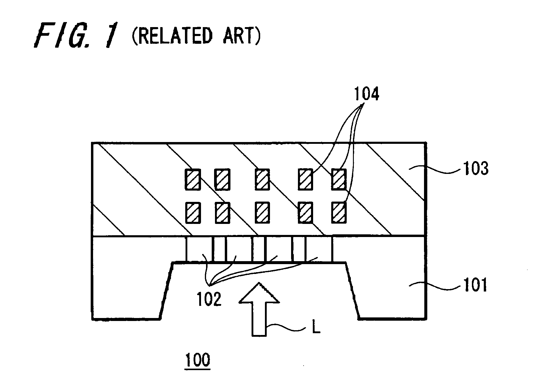
a solid-state imaging and manufacturing method technology, applied in solid-state devices, basic electric elements, radiation control devices, etc., can solve the problems of unstable interface of silicon substrate after grinding the back surface, insufficient light irradiation of photo sensor portions, and inability to achieve high yield ratio, excellent spectroscopic characteristics, and improved crystallinity on the interface of silicon layers

Inactive Publication Date: 2005-06-30
SONY CORP
View PDF3 Cites 95 Cited by
  • Summary
  • Abstract
  • Description
  • Claims
  • Application Information

AI Technical Summary

Benefits of technology

[0028] Furthermore, since the thickness of the silicon layer is thinner than the conventional ones, the distance between a lens and a semiconductor region of the photo sensor portion can be shortened.
[0056] Particularly, since the heat treatment at a comparatively low temperature can be performed for manufacturing, influences of the heat treatment to a transistor and others can be reduced, so that the transistor with a narrow pitch is formed to easily provide a minute pixel. Also, increase in the number of processes can be controlled.BRIEF DESCRIPTION OF THE DRAWINGS

Problems solved by technology

However, in a conventional CMOS image sensor in which light detection is performed by irradiating a photo sensor portion with light from a lens formed on a wiring portion through the space between wiring layers, the photo sensor portion can not be irradiated with an enough amount of light, because an eclipse of incident light due to the obstacle such as a wiring layer occurs and an aperture ratio of the photo sensor portion is made small in accordance with the high density integration of device to make the pixel become minute.
Accordingly, such problems as lower sensitivity and more shading may occur.
However, in the above-described manufacturing method, an interface of the silicon substrate after grinding the back surface becomes electrically unstable.
Also, a mechanical damage may affect the silicon substrate.
As a result, dark current is caused due to the above problems.
Hence, an image sensor of the back-illuminated type having the above-described structure has a limitation in use such as requiring a cooling process.
Furthermore, light absorption depends upon the thickness of a silicon layer; however, since the thickness is made thin by grinding, control for the thickness of the silicon layer (silicon substrate) of the photo sensor portion becomes deteriorated, so that the spectroscopic characteristic as the sensor tends to disperse.
As a result, the manufacturing yield ratio becomes deteriorated, and the cost may increase because of such a problem.
Accordingly, it is difficult to realize a minute pixel.

Method used


Image

  • Solid-state imaging device and method for manufacturing the same
  • Solid-state imaging device and method for manufacturing the same
  • Solid-state imaging device and method for manufacturing the same

Examples


Embodiment Construction

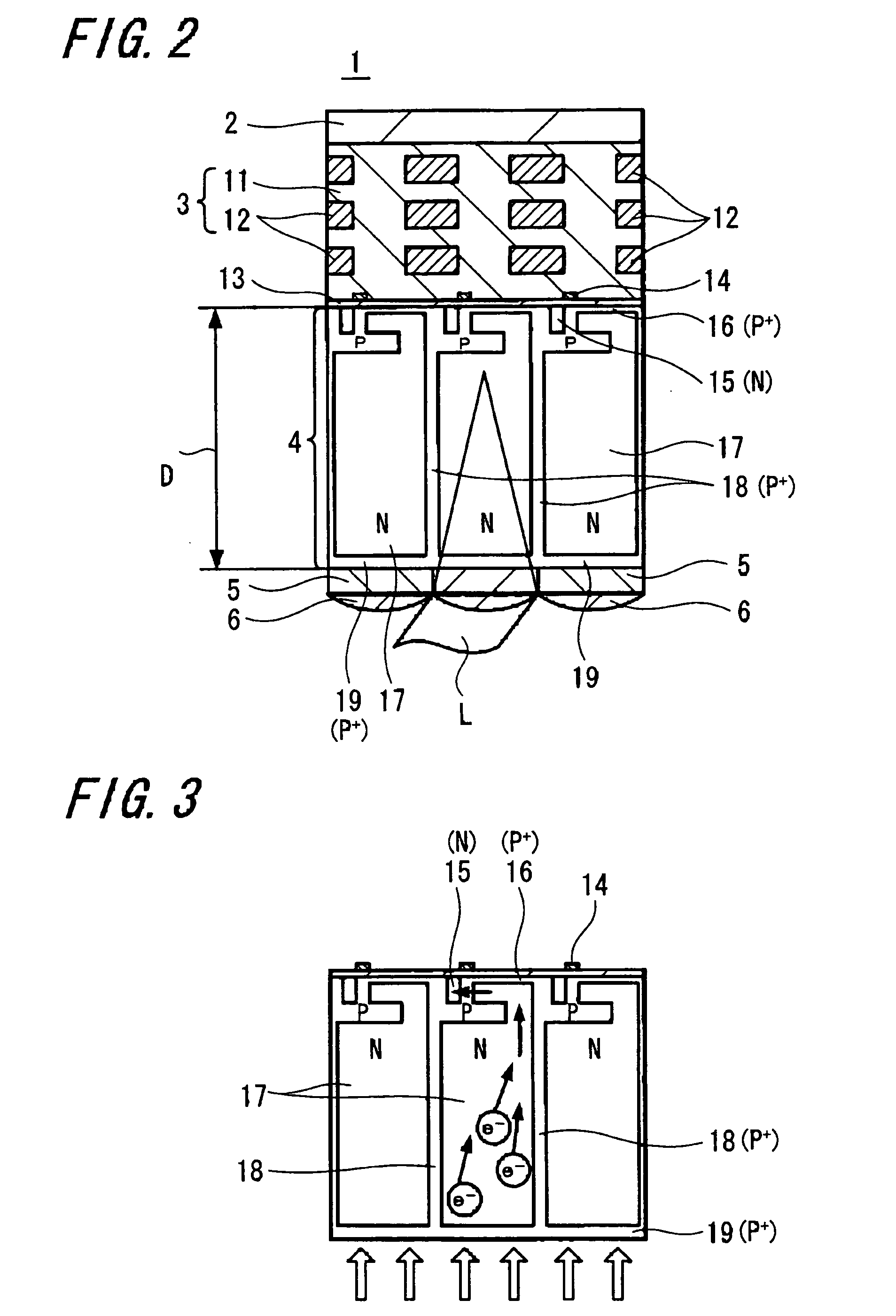
[0070]FIG. 2 shows a schematic constitutional view (showing a vertical section) of a solid-state imaging device of an embodiment of the present invention. In this embodiment, the present invention is applied to a CMOS image sensor (a CMOS type solid-state imaging device).

[0071] A solid-state imaging device 1 includes a supporting substrate 2, a wiring portion 3, a silicon substrate 4, a color filter 5 and an on-chip lens 6, which are formed from the front-surface side in this order.

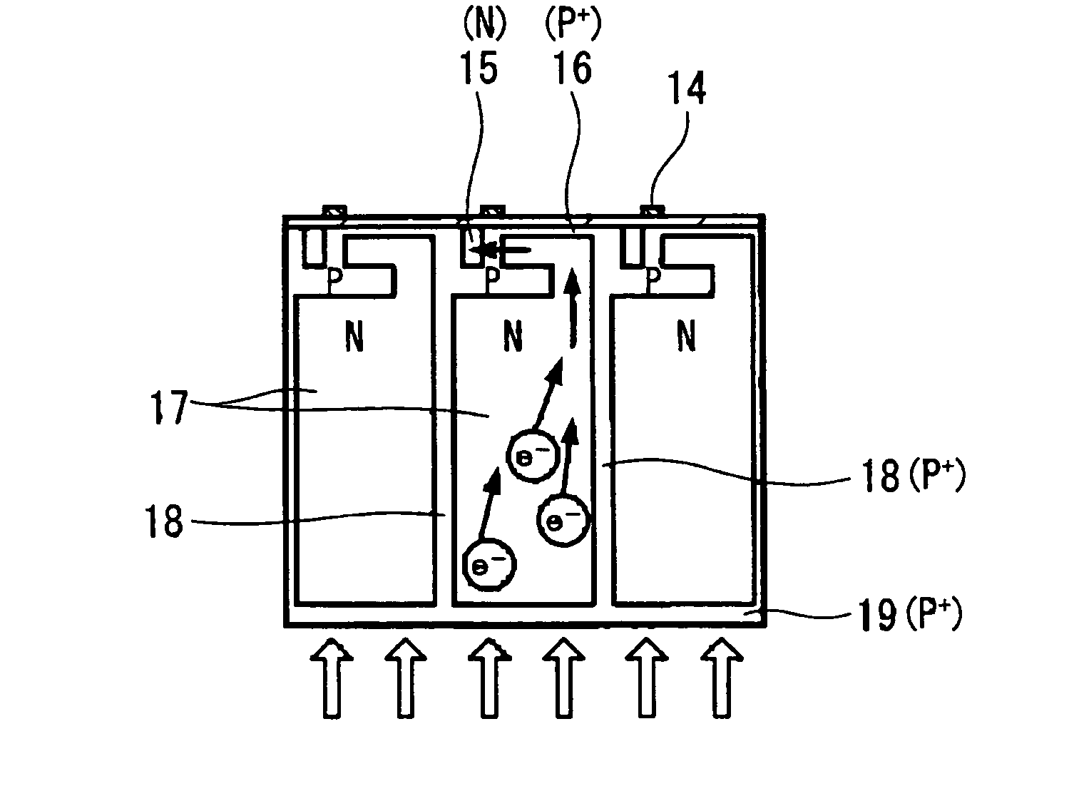
[0072] In the wiring potion 3, a plurality of wiring layers 12 are formed with an insulative layer 11 formed therebetween. A thin insulative coating 13 which functions as a gate insulative film is formed between the wiring portion 3 and the silicon substrate 4, and a gate electrode 14 is formed on the front-surface side of the insulative layer 13 for the read-out of the electric-charge.

[0073] An N-type region 17 constituting a photo diode of a photo sensor portion is formed in the silicon substrate thi...


PUM


Abstract

A solid-state imaging device having a high sensitivity and a structure in which a miniaturized pixel is obtained, and a method for manufacturing the solid-state imaging device in which an interface is stable, a spectroscopic characteristic is excellent and which can be manufactured with a high yield ratio are provided. The solid-state imaging device includes at least a silicon layer formed with a photo sensor portion and a wiring layer formed on the front-surface side of the silicon layer, and in which light L is made to enter from the rear-surface side opposite to the front-surface side of the silicon layer and the thickness of the silicon layer 4 is 10 μm or less. Also, the method for manufacturing the solid-state imaging device at least includes the steps of: forming a semiconductor region of a photo sensor portion in a silicon layer of a layered substrate in which a silicon substrate, an intermediate layer and a silicon layer are laminated; bonding a first supporting substrate onto the silicon layer; removing the silicon substrate and the intermediate layer; forming thereafter a wiring portion above the silicon layer; bonding a second supporting substrate onto the wiring portion, and removing the first supporting substrate to make the silicon layer exposed.

Description

BACKGROUND OF THE INVENTION [0001] 1. Field of the Invention [0002] The present invention relates to a solid-state imaging device and a method for manufacturing the same, and particularly relates to what is called a solid-state imaging device of a back-illuminated type and a method for manufacturing the same. [0003] 2. Description of the Related Art [0004] With a high density integration of a semiconductor device, a transistor and other semiconductor elements have been tried to be more miniaturized and to raise mounting density more than before. [0005] Therefore, in a CMOS image sensor (CMOS type solid-state imaging device), it is required that a pixel is made minute and an element is made to be highly integrated. [0006] However, in a conventional CMOS image sensor in which light detection is performed by irradiating a photo sensor portion with light from a lens formed on a wiring portion through the space between wiring layers, the photo sensor portion can not be irradiated with an...

Claims


Application Information

Patent Timeline
Patent Type & Authority Applications(United States)
IPC IPC(8): H01L27/14H01L21/00H01L23/00H01L27/146H01L29/74H01L31/00
CPCH01L27/14621H01L27/14625H01L27/14627H01L27/14636H01L27/14643H01L27/1464H01L27/14658H01L27/14683H01L27/14685H01L27/14689H01L27/14645H01L23/00H01L27/14
Inventor MARUYAMA, YASUSHIABE, HIDESHIMORI, HIROYUKI
Owner SONY CORP
Why Eureka
Try Eureka