Systems and methods for signal amplification with a dual-gate bio field effect transistor

a bio field effect transistor and signal amplification technology, applied in the field of systems and methods for signal amplification with a dual-gate bio field effect transistor, can solve problems such as fabrication and/or operation

Active Publication Date: 2013-08-08
TAIWAN SEMICON MFG CO LTD
View PDF13 Cites 87 Cited by
  • Summary
  • Abstract
  • Description
  • Claims
  • Application Information

AI Technical Summary

Problems solved by technology

While BioFETs are advantageous in many respects, challenges in their fabrication and / or operation arise, for example, due to compatibility issues between the semiconductor fabrication processes, the biological applications, restrictions and / or limits on the semiconductor fabrication processes, integration of the electrical signals and biological applications, and / or other challenges arising from implementing a large scale integration (LSI) process.

Method used


Image

  • Systems and methods for signal amplification with a dual-gate bio field effect transistor
  • Systems and methods for signal amplification with a dual-gate bio field effect transistor
  • Systems and methods for signal amplification with a dual-gate bio field effect transistor

Examples


Embodiment Construction

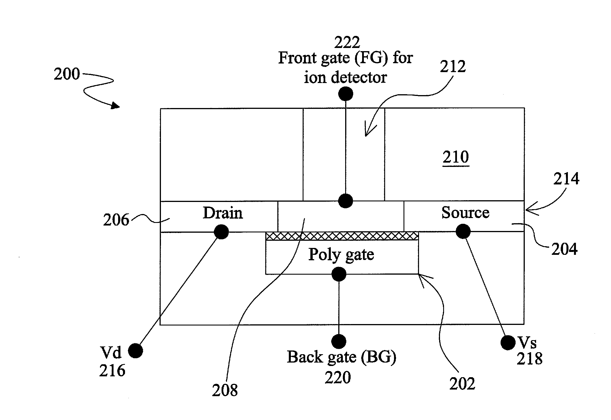
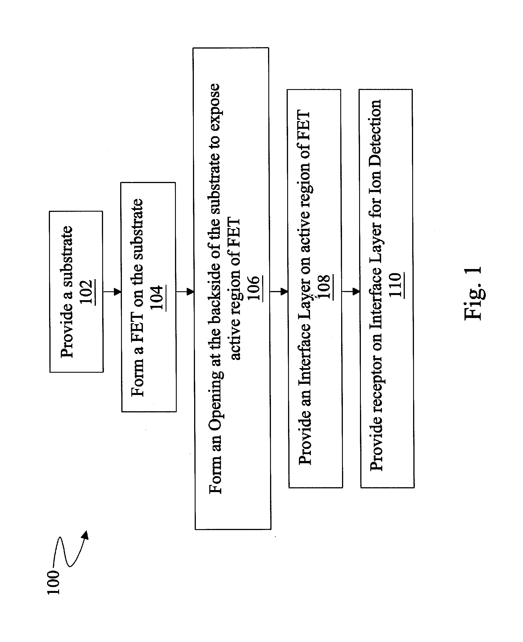
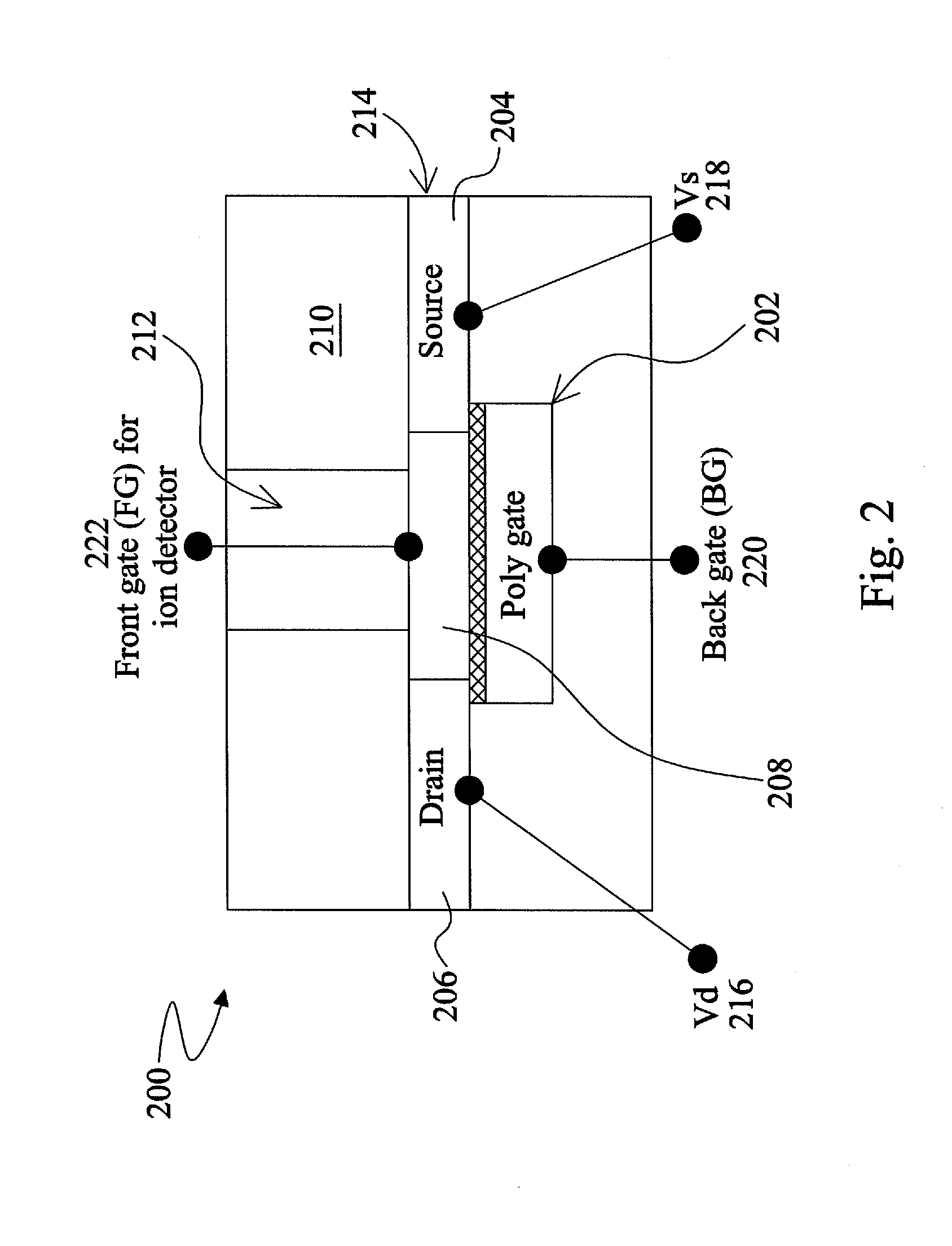
[0017]It is to be understood that the following disclosure provides many different embodiments, or examples, for implementing different features of the invention. Specific examples of components and arrangements are described below to simplify the present disclosure. These are, of course, merely examples and are not intended to be limiting. Moreover, the formation of a first feature over or on a second feature in the description that follows may include embodiments in which the first and second features are formed in direct contact, and may also include embodiments in which additional features may be formed interposing the first and second features, such that the first and second features may not be in direct contact. Further still, references to relative terms such as “top”, “front”, “bottom”, and “back” are used to provide a relative relationship between elements and are not intended to imply any absolute direction. Various features may be arbitrarily drawn in different scales for...


PUM

PropertyMeasurementUnit
energyaaaaaaaaaa
dielectric constantsaaaaaaaaaa
dielectric constantaaaaaaaaaa

Abstract

The present disclosure provides a bio-field effect transistor (BioFET) and a method of fabricating a BioFET device. The method includes forming a BioFET using one or more process steps compatible with or typical to a complementary metal-oxide-semiconductor (CMOS) process. The BioFET device may include a substrate; a gate structure disposed on a first surface of the substrate and an interface layer formed on the second surface of the substrate. The interface layer may allow for a receptor to be placed on the interface layer to detect the presence of a biomolecule or bio-entity. An amplification factor of the BioFET device may be provided by a difference in capacitances associated with the gate structure on the first surface and with the interface layer formed on the second surface.

Description

PRIORITY DATA[0001]This application claims priority to Non-Provisional application Ser. No. 13 / 480,161, filed on May 24, 2012, entitled “CMOS COMPATIBLE BIOFET”, which claims priority to Provisional Application Ser. No. 61 / 553,606, filed on Oct. 31, 2011, entitled “CMOS COMPATIBLE BIOFET”. The entire contents of these applications are hereby incorporated by reference herein.BACKGROUND[0002]Biosensors are devices for sensing and detecting biomolecules and operate on the basis of electronic, electrochemical, optical, and mechanical detection principles. Biosensors that include transistors are sensors that electrically sense charges, photons, and mechanical properties of bio-entities or biomolecules. The detection can be performed by detecting the bio-entities or biomolecules themselves, or through interaction and reaction between specified reactants and bio-entities / biomolecules. Such biosensors can be manufactured using semiconductor processes, can quickly convert electric signals, a...

Claims


Application Information

Patent Timeline
Patent Type & Authority Applications(United States)
IPC IPC(8): G01N27/414H01L29/66
CPCG01N27/414G01N27/4145H01L29/66477G01N27/4148H10K85/761H01L29/66484H01L29/7831H01L29/78648
Inventor LIU, YI-SHAOBASHIR, RASHIDLAI, FEI-LUNGCHENG, CHUN-WEN
Owner TAIWAN SEMICON MFG CO LTD
Why Eureka
Try Eureka