Transparent conductive film, method of producing the same, photoelectric conversion apparatus, and electronic apparatus
a technology of transparent conductive film and photoelectric conversion apparatus, which is applied in the direction of conductive layers on insulating supports, sustainable manufacturing/processing, and final product manufacturing, etc., can solve the problems of high installation cost of sputtering apparatus, long takt time, and inability to secure conductivity in other parts than the metal fine line portion, etc., to achieve high visible light transmittance, low sheet resistance, and high conductivity
Inactive Publication Date: 2013-08-15
SONY CORP
View PDF16 Cites 24 Cited by
- Summary
- Abstract
- Description
- Claims
- Application Information
AI Technical Summary
Benefits of technology
[0063]According to the present technology, it is possible to achieve a transparent conductive film that has sufficiently low sheet resistance and a sufficiently high visible light transmittance, is capable of securing high conductivity on an entire surface thereof, and has excellent corrosion resistance to an electrolyte solution. Moreover, it is possible to easily produce such a transparent conductive film at low costs. Moreover, by using the transparent conductive film as, for example, a transparent conductive film of a photoelectric conversion apparatus that uses an electrolyte solution, such as a dye-sensitized photoelectric conversion apparatus, it is possible to improve corrosion resistance to an electrolyte solution of the transparent conductive film, which improves the life-span of the photoelectric conversion apparatus. Moreover, it is possible to achieve a photoelectric conversion apparatus with high performance. Furthermore, by using the transparent conductive film as a transparent conductive film of an electronic apparatus, it is possible to achieve an electronic apparatus with high performance.
Problems solved by technology
Therefore, there is a problem in that not only the installation cost of a sputtering apparatus is high but also the takt time is long.
However, there are problems in that it is impossible to secure conductivity in portions other than the metal fine line portion, and the metal fine line portion is easily corroded if the metal fine line portion is directly brought into contact with, for example, an electrolyte solution including iodine and the like.
However, in a case where a two-dimensional material such as a carbon nanotube and a metal nanowire is used as a transparent conductive film (e.g., see Patent Document 2), it is difficult to completely coat the metal fine line network layer while maintaining high transparency.
This causes a problem of corrosion due to an electrolyte solution.
Although the most promising transparent conductive film is an oxide thin film including ITO or the like, the oxide thin film has various problems.
First, because film formation by means of a sputtering method is needed to produce a transparent conductive film with high quality, it takes a lot of cost inevitably.
Second, because a transparent conductive film includes oxide, it has less flexibility and it is difficult to apply it to a flexible substrate and the like.
Third, for example, because ITO with high conductivity has less thermal stability and less corrosion resistance, it cannot be used for a transparent conductive film such as a dye-sensitized solar cell.
Fourth, it is difficult for a transparent oxide thin film to satisfy conditions such as corrosion resistance, transparent conductivity, flexibility, and simplicity of a manufacturing process, in view of its structure.
Method used
View moreImage
Smart ImageViewing Examples

Examples
first embodiment (
1. First Embodiment (transparent conductive film and method of producing the same)
second embodiment (
2. Second Embodiment (transparent conductive film and method of producing the same)
third embodiment (
3. Third embodiment (transparent conductive film and method of producing the same)
Login to view more PUM
| Property | Measurement | Unit |
|---|---|---|
| light transmittance | aaaaa | aaaaa |
| smoothness | aaaaa | aaaaa |
| thickness | aaaaa | aaaaa |
Abstract
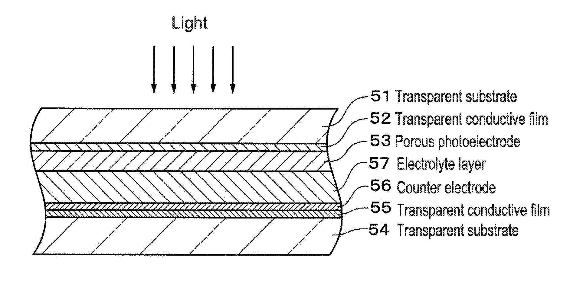
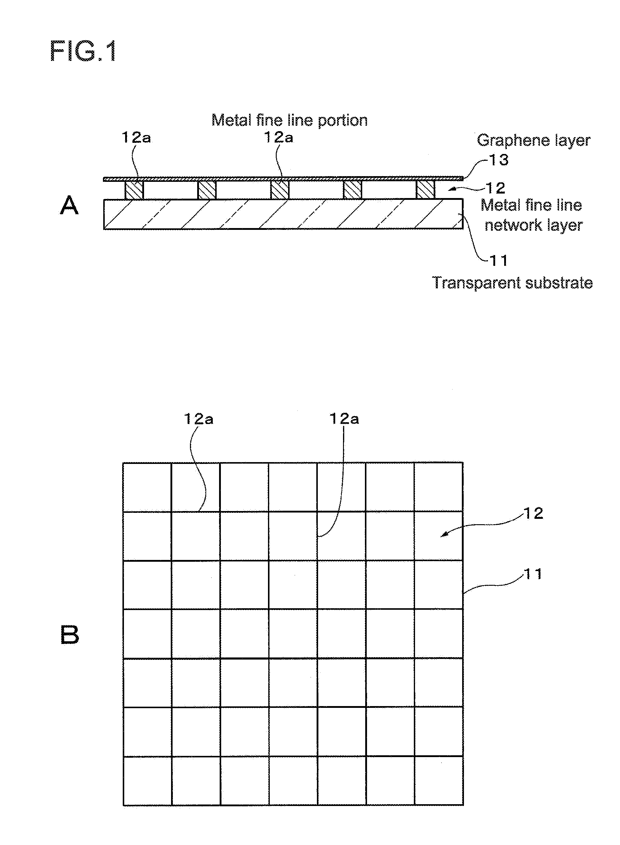
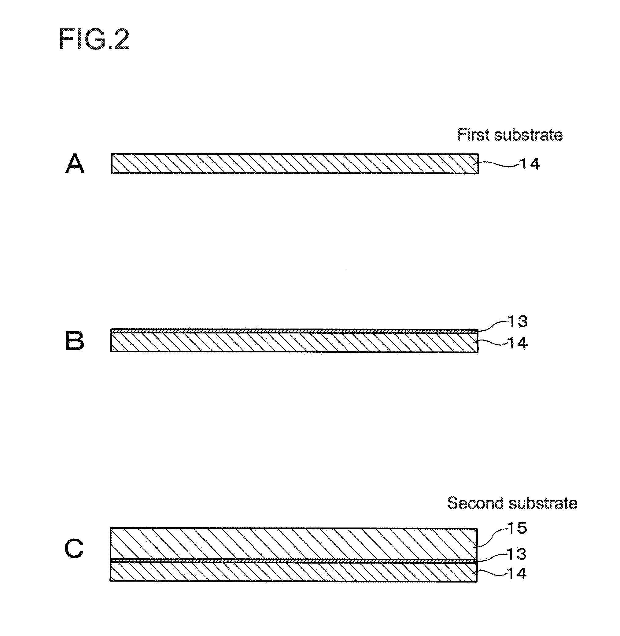
[Object] To provide a transparent conductive film that has sufficiently low sheet resistance and a sufficiently high visible light transmittance, is capable of securing high conductivity on an entire surface thereof, and has excellent corrosion resistance to an electrolyte solution, a method of producing the transparent conductive film, and a photoelectric conversion apparatus and an electronic apparatus using the transparent conductive film.[Solving Means] A transparent conductive film includes a metal fine line network layer 12 and one or more layers of graphene layers 13 provided on at least one surface of the metal fine line network layer 12. The metal fine line network layer 12 includes at least one metal selected from a group consisting of copper, silver, aluminum, gold, iron, nickel, titanium, and platinum. The metal fine line network layer 12 is provided on a transparent substrate 11. In order to achieve a flexible transparent conductive film, a transparent plastic substrate is used as the transparent substrate 11.
Description
TECHNICAL FIELD[0001]The present technology relates to a transparent conductive film, a method of producing the transparent conductive film, a photoelectric conversion apparatus, and an electronic apparatus, and is suitable for use in a transparent conductive film that is used for a display, a touch panel, a dye-sensitized solar cell, and the like.BACKGROUND ART[0002]In order to increase the area of a display, to make a solar cell more efficient, to make a touch panel more large and fine, and the like, there is a need for a transparent conductive film with low sheet resistance. At present, there are three main structures, which are used for a transparent conductive film with low resistance or a transparent conductive sheet.[0003]The first of these is a transparent oxide thin film typified by an indium-tin oxide (ITO). The transparent oxide thin film needs to be formed by means of a sputtering method. Therefore, there is a problem in that not only the installation cost of a sputterin...
Claims
Login to view more Application Information
Patent Timeline
 Patent Type & Authority Applications(United States)
IPC IPC(8): H01B1/04H01G9/20H01B13/00
CPCH01G9/2022H01G9/2031H01G9/2059H01L51/445Y02E10/542B82Y40/00H01B1/04H01B13/0036C01B31/0453B82Y30/00Y02E10/549C01B32/186Y02P70/50H10K30/83H01B5/14H01B13/00H01L31/04H01M14/00
Inventor SHIMIZU, KEISUKEKOBAYASHI, TOSHIYUKI
Owner SONY CORP
- R&D Engineer
- R&D Manager
- IP Professional
Why Eureka
- Industry Leading Data Capabilities
- Powerful AI technology
- Patent DNA Extraction
Try Eureka
Browse by: Latest US Patents, China's latest patents, Technical Efficacy Thesaurus, Application Domain, Technology Topic.
© 2024 PatSnap. All rights reserved.Legal|Privacy policy|Modern Slavery Act Transparency Statement|Sitemap