

Display device
- Summary
- Abstract
- Description
- Claims
- Application Information
AI Technical Summary
Benefits of technology
Problems solved by technology
Method used
Image

Examples
first embodiment
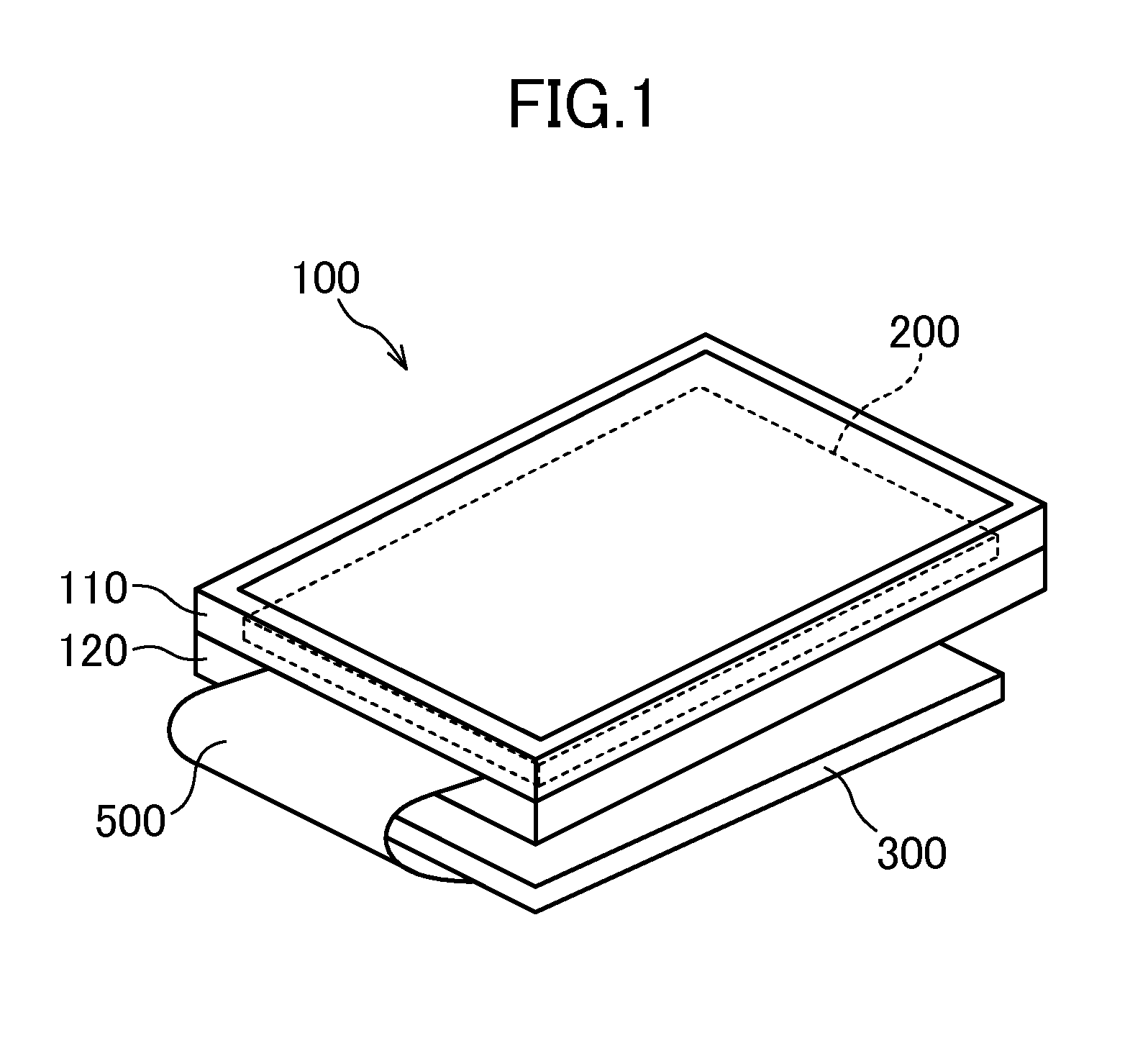
[0031]FIG. 1 is a diagram illustrating a display device 100 according to a first embodiment of the present invention. In this example, the display device 100 according to this embodiment is a liquid crystal display device, but may be any display device such as an organic EL (electro-luminescent) display device if a driver circuit element is arranged on a glass substrate to conduct a display control. As illustrated in FIG. 1, the display device 100 includes an upper frame 110 and a lower frame 120 which are fixed to sandwich a display panel 200, an image signal control unit 300 that converts image information into a format that can be displayed on the display panel 200 according to a command from a main control unit not shown, and a flexible printed circuit (FPC) 500 that transmits the information converted in the image signal control unit 300 to the display panel 200.
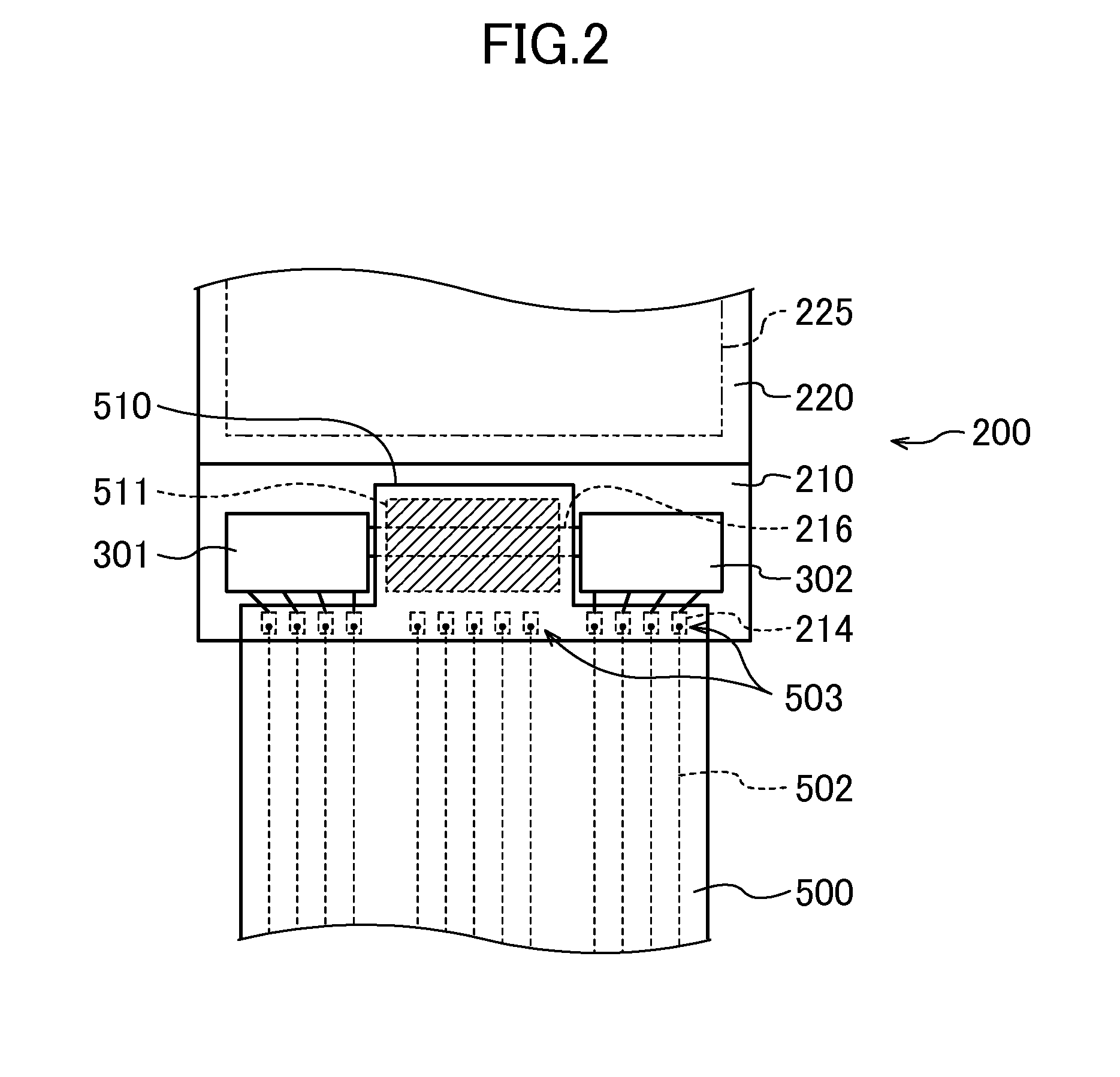
[0032]FIG. 2 is a diagram illustrating a neighborhood of a connection portion between the display panel 200 and the f...
second embodiment
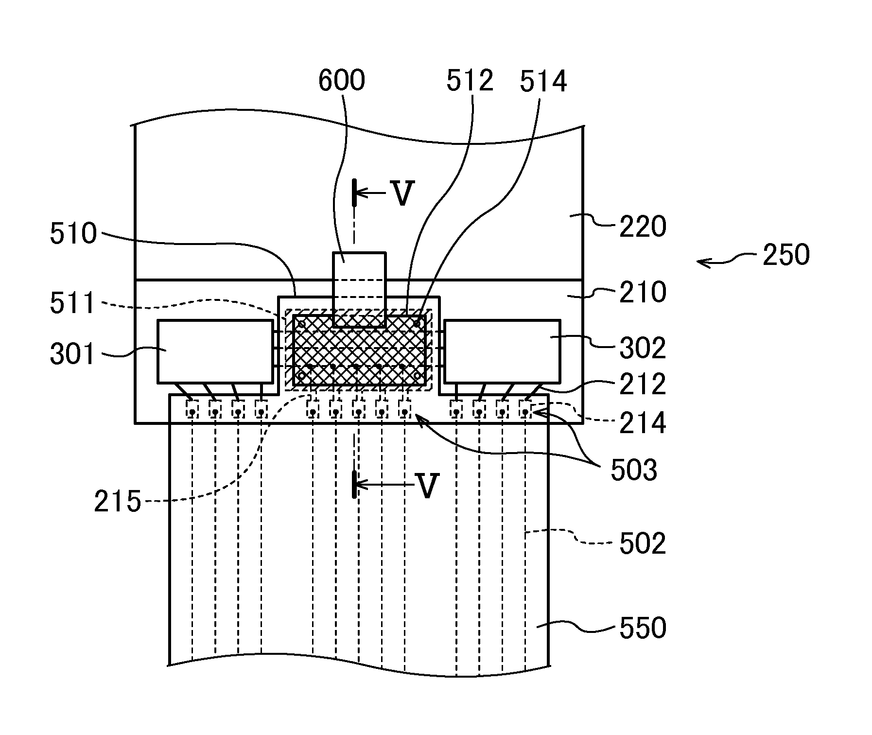
[0037]FIG. 4 is a diagram illustrating a neighborhood of a connection portion between a display panel 250 and a flexible printed circuit 550 in a display device according to a second embodiment of the present invention in detail. FIG. 5 is a cross-sectional view taken along a line V-V in FIG. 4. The display device according to the second embodiment is substantially identical with that in the above-mentioned modified example of the first embodiment illustrated in FIG. 3. Differences from the modified example of the first embodiment reside in that a front surface conductive pattern 512 which is a conductive pattern is disposed on a front surface side of the electromagnetic wave blocking portion 510, which does not face the TFT substrate 210, the front surface conductive pattern 512 and the rear surface conductive pattern 511 are electrically connected to each other through through-holes 514, and the front surface conductive pattern 512 is connected to the ground potential line of the ...
third embodiment
[0039]FIG. 6 is a diagram illustrating a neighborhood of a connection portion between a display panel 260 and a flexible printed circuit 560 in a display device according to a third embodiment of the present invention in detail. This embodiment is different from the second embodiment in that the front surface conductive pattern 512 of the second embodiment is not provided, but the electromagnetic wave blocking portion 510 and the rear surface conductive pattern 511 are further extended in a direction of the display area, and connected to the ground potential line of the color filter substrate 220. Other configurations are identical with those in the second embodiment. Even with this configuration, the electromagnetic waves occurring in the inter-driver signal lines 216 can be blocked by the rear surface conductive pattern 511 of the electromagnetic wave blocking portion 510. Also, the ground potential of the master driver circuit element 301 and the slave driver circuit element 302,...
PUM
 Abstract
Description
Claims
Application Information