Light-emitting display device

Inactive Publication Date: 2010-04-22
SEMICON ENERGY LAB CO LTD
View PDF99 Cites 22 Cited by
  • Summary
  • Abstract
  • Description
  • Claims
  • Application Information

AI Technical Summary

Benefits of technology

[0024]A light-emitting transistor which has high reliability and high mobility can be formed.
[0025]Further, an active layer of a switching transistor and a pixel electrode can be formed using the same mask, which leads to reduction of the number of masks.
[0026]Furthermore, in a ligh

Problems solved by technology

As for a light-emitting display device in which a TFT including an oxide semiconductor film, which has high electric field mobility, and a light-emitting element in which light emission is obtained by recombination of electrons and holes i

Method used


Image

  • Light-emitting display device
  • Light-emitting display device
  • Light-emitting display device

Examples


Example

Embodiment 1

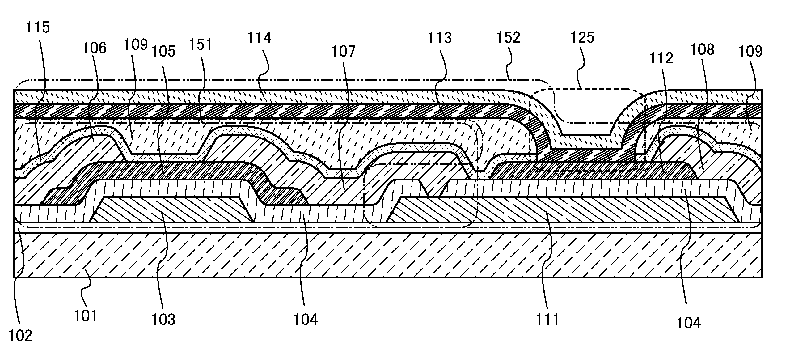
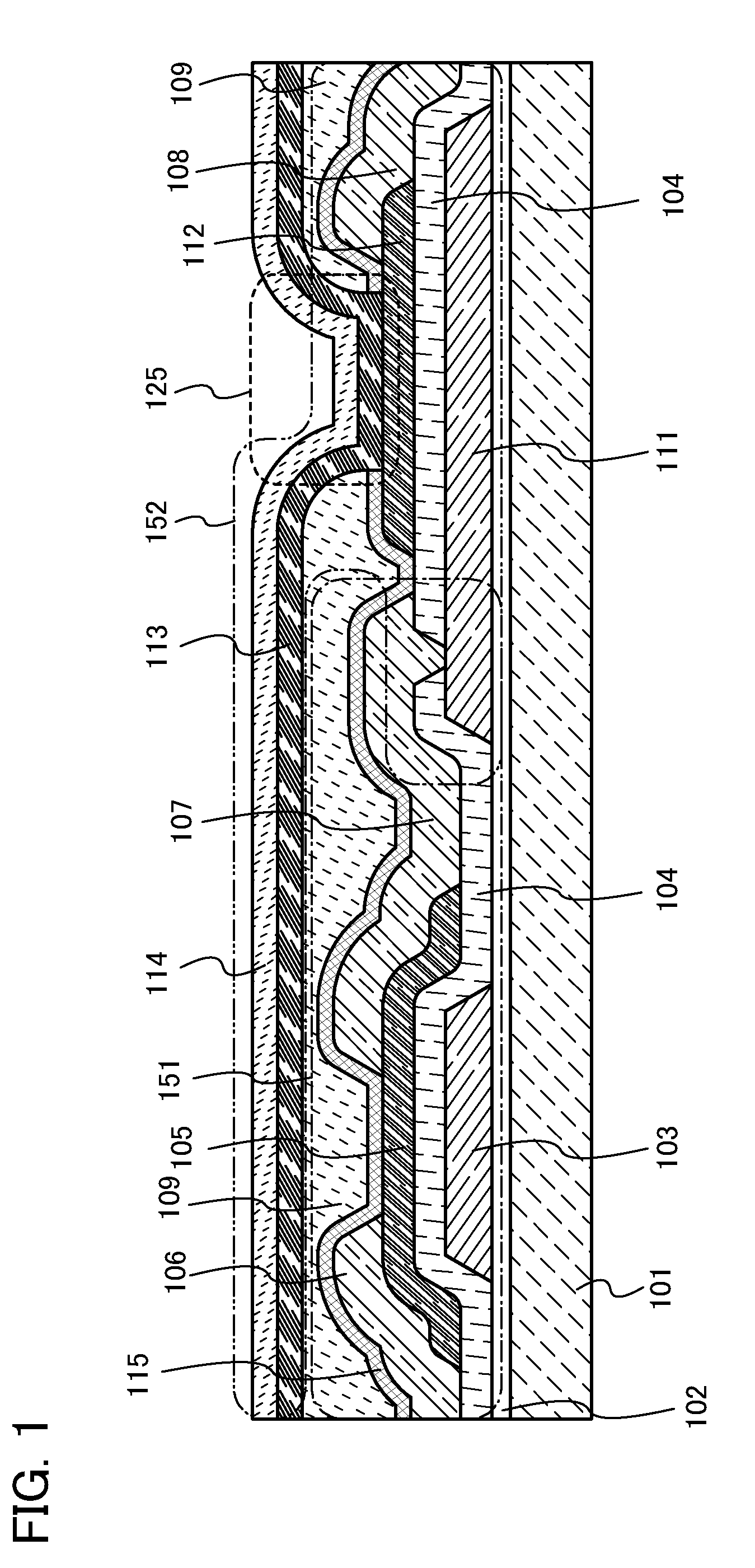
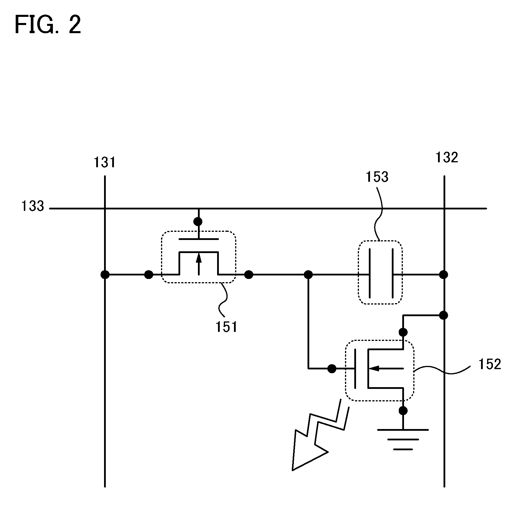
[0039]Embodiment 1 will now be described with reference to FIG. 1, FIG. 2, FIGS. 3A to 3C, FIGS. 4A to 4C, FIGS. 5A to 5C, FIGS. 6A to 6C, FIGS. 7A and 7B, FIGS. 8A and 8B, and FIG. 9.

[0040]A base film 102 and a conductive film 124 are formed first over a substrate 101 (FIG. 3A).

[0041]In FIG. 3A, as the substrate 101, it is possible to use a glass substrate made of barium borosilicate glass, aluminoborosilicate glass, or the like typified by 7059 glass, 1737 glass, or the like manufactured by Corning Incorporated.

[0042]For the base film 102, a silicon oxide film, a silicon nitride oxide film, a silicon nitride film, or a silicon oxynitride film may be used. In addition, an insulating film 104 is formed later, and thus the base film 102 is not necessarily formed, if not needed. In this embodiment, a silicon oxide film is used as the base film 102.

[0043]The conductive film 124 is preferably formed using a conductive material having low resistance, such as aluminum (Al) or ...


PUM


Abstract

The light-emitting display device comprises first and second thin film transistors. The first thin film transistor includes a first gate electrode; a first oxide semiconductor film; and a first electrode and a second electrode which are electrically connected to the first oxide semiconductor film. The second thin film transistor includes a second gate electrode electrically connected to the second electrode; a second oxide semiconductor film; a third electrode; a light-emitting layer and a fourth electrode over the second oxide semiconductor film. A work function of the second oxide semiconductor film is higher than a work function of the fourth electrode.

Description

BACKGROUND OF THE INVENTION[0001]1. Field of the Invention[0002]The present invention in this specification relates to a light-emitting display device in which an oxide semiconductor is used and a method for manufacturing the light-emitting display device.[0003]2. Description of the Related Art[0004]It has been promoted to develop light-emitting elements where electrons are injected from one electrode and holes are injected from the other electrode into a stacked body containing an organic compound sandwiched between the pair of electrodes and the electrons and holes are recombined in the stacked body so that a light-emitting material in the stacked body is excited and thus light emission can be obtained. Further, development of light-emitting devices and display devices using the light-emitting elements has been also promoted.[0005]Being self-light-emitting type ones, such light-emitting elements are superior in visibility with low dependence on a viewing angle, and thin shape and ...

Claims


Application Information

Patent Timeline
IPC IPC(8): H01L33/00H05B44/00
CPCH01L29/7869H01L27/1225H01L29/78633H10K59/126
Inventor GODO, HIROMICHI
Owner SEMICON ENERGY LAB CO LTD
Why Eureka
Try Eureka