Method for manufacturing active array substrate

Active Publication Date: 2013-08-15
E INK HLDG INC
View PDF1 Cites 4 Cited by
  • Summary
  • Abstract
  • Description
  • Claims
  • Application Information

AI Technical Summary

Benefits of technology

[0006]A purpose of the disclosure is to provide a method for manufacturing an active array substrate by using only two photolithography process steps, and the act

Problems solved by technology

Generally, a method for manufacturing the active array substrate needs to cond

Method used


Image

  • Method for manufacturing active array substrate
  • Method for manufacturing active array substrate
  • Method for manufacturing active array substrate

Examples


Embodiment Construction

[0013]The disclosure is described by the following specific embodiments. Those with ordinary skill in the arts can readily understand the other advantages and functions of the present invention after reading the disclosure of this specification. The disclosure can also be implemented with different embodiments. Various details described in this specification can be modified based on different viewpoints and applications without departing from the scope of the disclosure.

[0014]Reference will now be made in detail to the present embodiments of the disclosure, examples of which are illustrated in the accompanying drawings. Wherever possible, the same reference numbers are used in the drawings and the description to refer to the same or like parts.

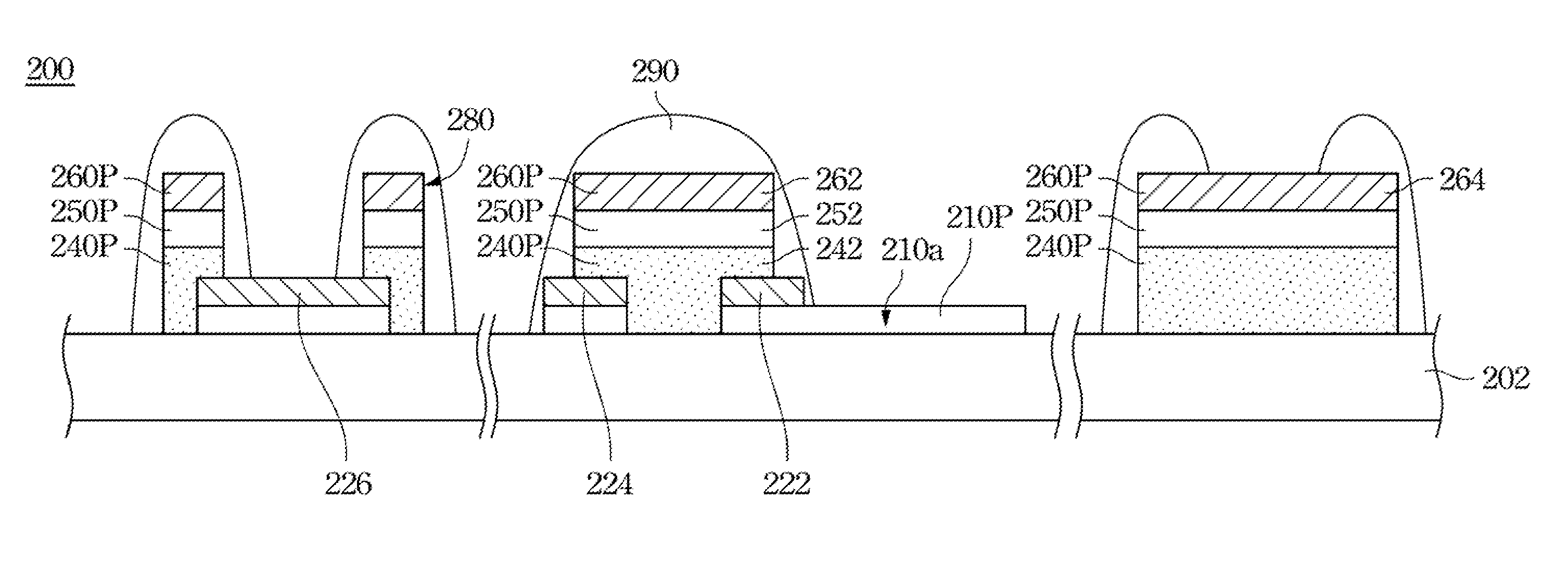
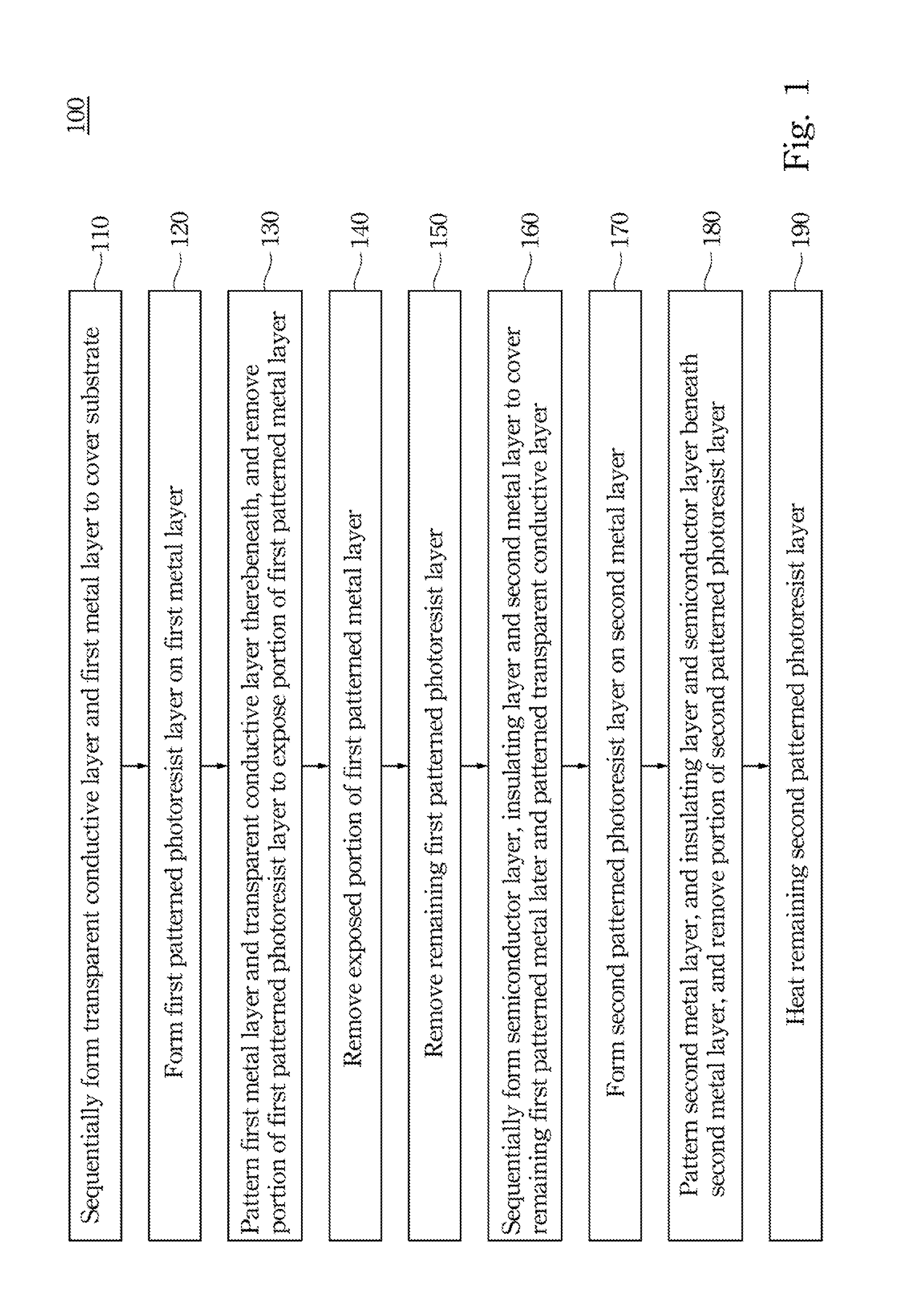
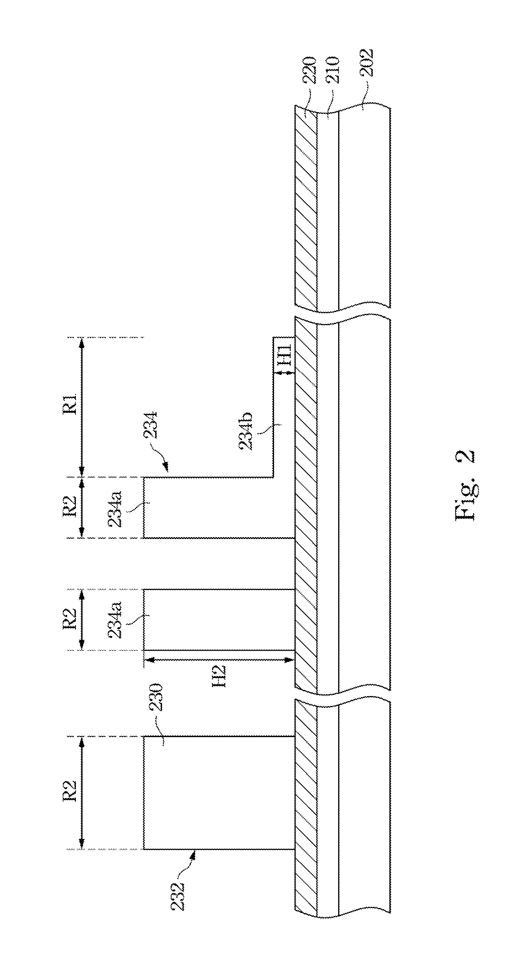
[0015]FIG. 1 is a flow chart schematically illustrating a method 100 for manufacturing an active array substrate according to one embodiment of the disclosure. FIGS. 2, 3, 4, 5, 6A and 7 are cross-sectional views schematically illustrating pro...


PUM


Abstract

A method for manufacturing an active array substrate is provided herein. The active array substrate can be manufactured by using only two photolithography process steps. The photolithography process step using a first photomask may be provided for forming a drain electrode, a source electrode, a data line and/or a data line connecting pad and a patterned transparent conductive layer, etc. The photolithography process step using a second photomask may be utilized for forming a gate electrode, a gate line, a gate insulating layer, a channel layer and/or a gate line connecting pad, and so forth.

Description

RELATED APPLICATIONS[0001]This application claims priority to Taiwan Application Serial Number 10104428 filed Feb. 10, 2012, which is herein incorporated by reference.BACKGROUND[0002]1. Technical Field[0003]The present disclosure relates to a method for manufacturing an active array substrate.[0004]2. Description of Related Art[0005]A flat panel display device such as a liquid crystal display device has been widely applied in a variety of electronic products. The flat panel display device typically includes an active array substrate for driving pixels in the flat panel display device. Generally, a method for manufacturing the active array substrate needs to conduct five photolithography process steps each of which consumes production cost. In recent years, in order to economically produce the active array substrate, a manufacturing method using four photolithography process steps has been developed in this industry so as to efficiently produce the active array substrate. However, th...

Claims


Application Information

Patent Timeline
IPC IPC(8): H01L21/8234
CPCH01L27/1288
Inventor TANG, WEN-CHUNGSHU, FANG-ANTSAI, YAO-CHOUSHINN, TED-HONG
Owner E INK HLDG INC
Why Eureka
Try Eureka