Light field imaging device and image processing device

Active Publication Date: 2013-08-22
PANASONIC INTELLECTUAL PROPERTY MANAGEMENT CO LTD
View PDF11 Cites 103 Cited by
  • Summary
  • Abstract
  • Description
  • Claims
  • Application Information

AI Technical Summary

Benefits of technology

[0019]According to an embodiment of the present invention, an image can be captured so as to be focused on the imaging area of the image sensor and image information represented by the light that has been incident on one of the two light-transmitting areas can be

Problems solved by technology

According to such a so-called “two-lens image capturing” technique, however, two cameras need to be used, thus increasing not only the overall size of the image capture device but also the manufacturing cost as well.
But its resolution is determined by the number of micro lenses and should be lower than the resolution determined by the number of pixels of the image sensor, which is a pr

Method used


Image

  • Light field imaging device and image processing device
  • Light field imaging device and image processing device
  • Light field imaging device and image processing device

Examples


embodiment 1

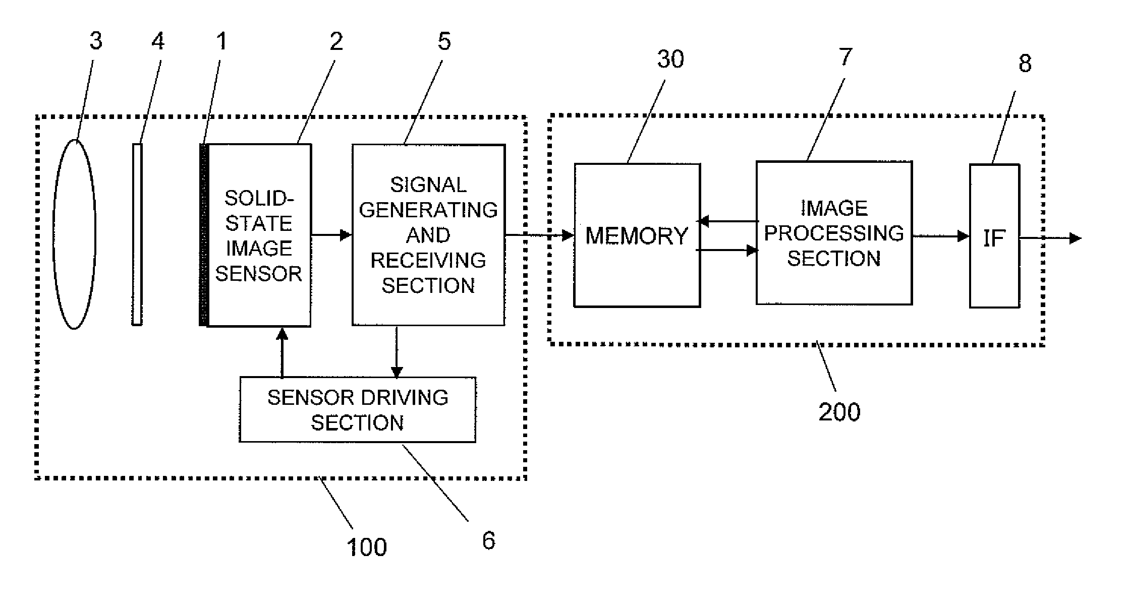
[0051]First of all, an image capture device as a first embodiment of the present invention will be described. FIG. 1 is a block diagram illustrating a general configuration for a light field image capture device according to this embodiment (which will be simply referred to herein as an “image capture device”). The image capture device of this embodiment is a digital electronic camera and includes an image capturing section 100 and a signal processing section 200 that generates a signal representing an image (i.e., an image signal) based on the signal generated by the image capturing section 100.

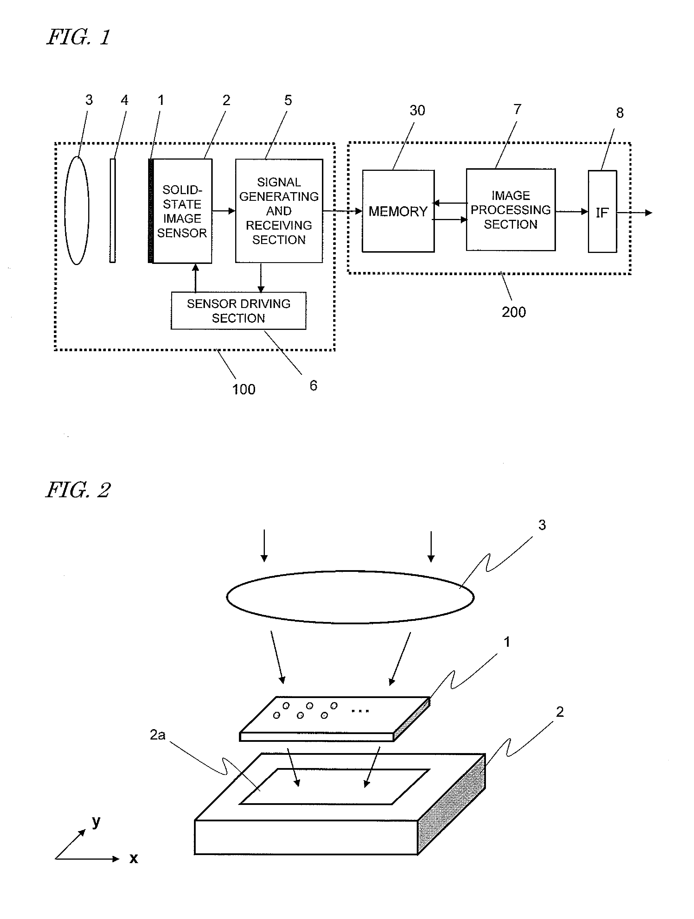
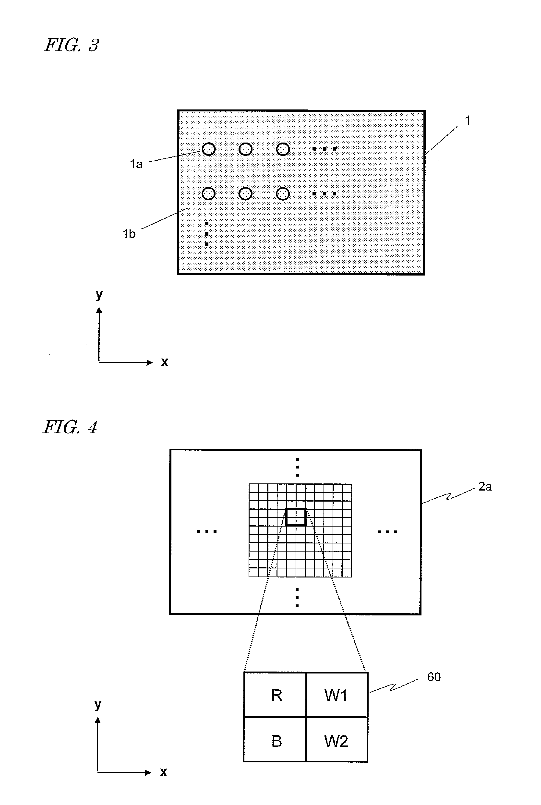
[0052]The image capturing section 100 includes a color solid-state image sensor 2 (which will be simply referred to herein as an “image sensor”) with a number of photosensitive cells that are arranged on its imaging area, a light-transmitting plate (light-transmitting section) 1 with two light-transmitting areas, which the respective transmittances have mutually different wavelength dependen...

embodiment 2

[0089]Next, a second embodiment of the present invention will be described. This second embodiment is the same as the first embodiment described above except that the optical lens 3 and the image sensor 2 of this embodiment have a different basic color scheme from that of the first embodiment. Thus, the following description of the second embodiment will be focused on that difference from the first embodiment and their common features will not be described all over again.

[0090]FIG. 7 illustrates how the incoming light is imaged by the optical lens 3 of this embodiment. In this embodiment, the optical lens 3 has different focal lengths on its peripheral portion 3a and its central portion 3b. Specifically, the lens peripheral portion 3a has a relatively short focal length and the lens central portion 3b has a relatively long focal length. With such a property taken into account, the optical lens 3, the light-transmitting plate 1 and the image sensor 2 are arranged so that the light th...

embodiment 3

[0096]Next, a third embodiment of the present invention will be described. In this embodiment, two kinds of light-transmitting members, of which the spectral transmittance characteristics are the same as those of the two kinds of light-transmitting areas of the light-transmitting plate 1, are arranged in front of the light incident surface (i.e., its front surface) of the optical lens 3 of the second embodiment. Specifically, as shown in FIG. 9, a light-transmitting member 1aa having the same spectral transmittance characteristic as the light-transmitting areas 1a of the light-transmitting plate 1 is arranged in front of the peripheral portion 3a of the lens 3, and a light-transmitting member 1bb having the same spectral transmittance characteristic as the light-transmitting area 1b of the light-transmitting plate 1 is arranged in front of the central portion 3b of the lens 3. In the other respects, the configuration and processing of this third embodiment are the same as those of t...


PUM


Abstract

This image capture device includes: an image sensor 2 including first and second types of pixels that have mutually different spectral transmittance characteristics; a light-transmitting section 1 that is arranged to face the imaging area of the image sensor 2; and an imaging section 3 that includes at least a first imaging area having a first focal length and a second imaging area having a second focal length that is longer than the first focal length. The light-transmitting section 1 has a first light-transmitting area 1a comprised of multiple partial areas that are separated from each other and a second light-transmitting area 1b having a different spectral transmittance characteristic from the first light-transmitting area 1a. The distance from the light-transmitting section 1 to the imaging section 3 is equal to the first focal length f1 and the distance from the imaging area of the image sensor 2 to the imaging section 3 is equal to the second focal length f2.

Description

TECHNICAL FIELD[0001]The present application relates to a single-lens 3D image capturing technology for generating a multi-viewpoint image using a single optical system and a single image sensor.BACKGROUND ART[0002]Recently, the performance and functionality of digital cameras and digital movie cameras that use some solid-state image sensor such as a CCD or a CMOS (which will be sometimes simply referred to herein as an “image sensor”) have been enhanced to an astonishing degree. In particular, the size of a pixel structure for use in an image sensor has been further reduced these days thanks to rapid development of semiconductor device processing technologies, thus getting an even greater number of pixels and drivers integrated together in an image sensor. As a result, the resolution of an image sensor has lately increased rapidly from around one million pixels to ten million or more pixels in a matter of few years. On top of that, the quality of an image captured has also been imp...

Claims


Application Information

Patent Timeline
IPC IPC(8): H04N13/02H04N13/271
CPCG02B27/0075G02B3/00G06T7/0065H04N5/225G06T2207/10052H04N9/045H04N13/0217H04N13/0271G03B35/10H04N13/02G06T7/557H04N13/20H04N13/218H04N13/271H04N23/957H04N23/00H04N25/134
Inventor HIRAMOTO, MASAOISHII, YASUNORI
Owner PANASONIC INTELLECTUAL PROPERTY MANAGEMENT CO LTD
Why Eureka
Try Eureka