

High speed high density connector assembly
- Summary
- Abstract
- Description
- Claims
- Application Information
AI Technical Summary
Benefits of technology
Problems solved by technology
Method used
Image


Examples
first embodiment
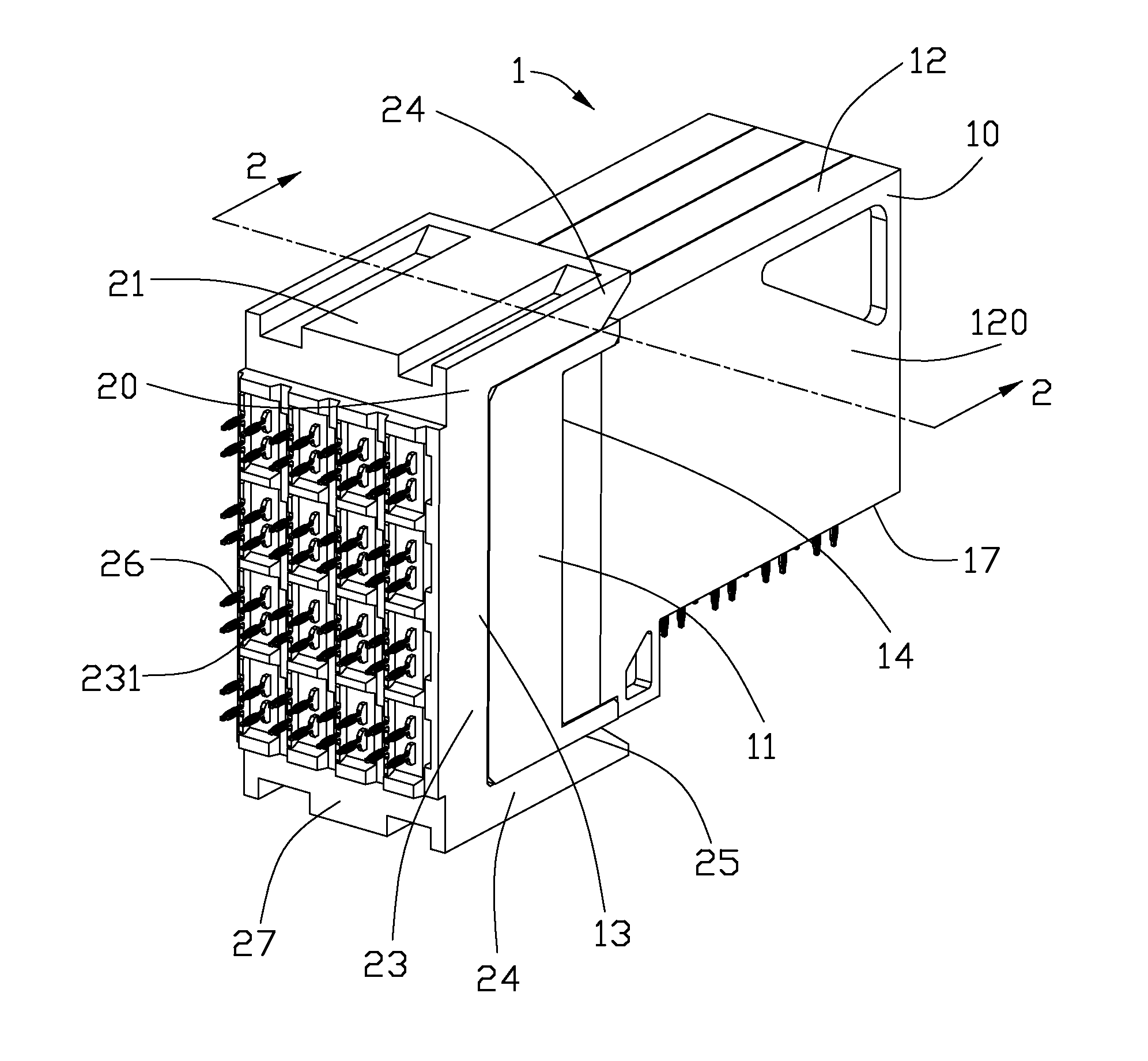
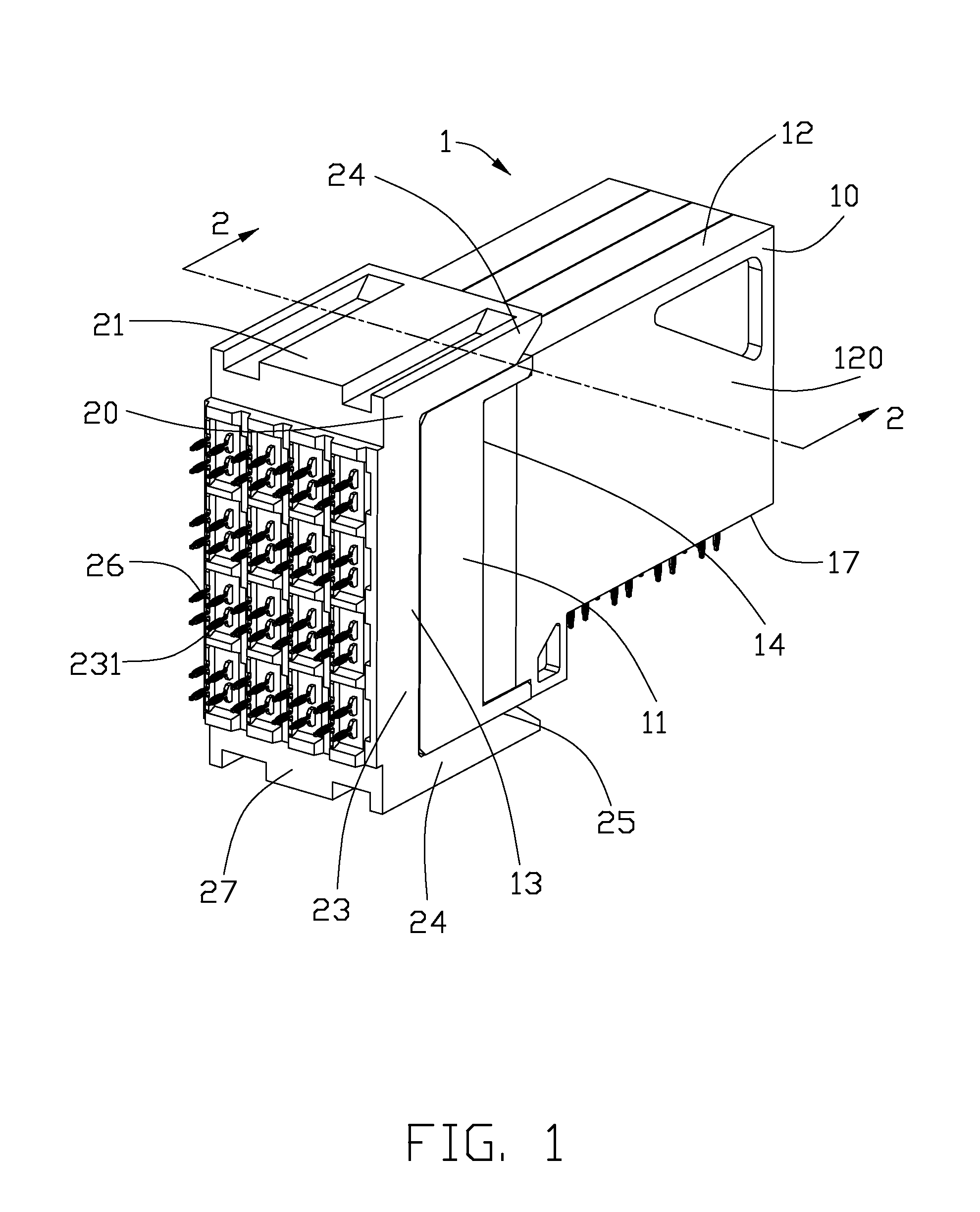
[0031]FIGS. 1-4 show a connector assembly according to present invention. The connector assembly 1 is shown to connect a daughter card (not shown) to a backplane (not shown). The connector assembly 1 includes a plug 10 mounted onto the daughter card and a header 20 mounted onto the backplane.
[0032]The plug 10 includes a conductive front housing 11 and a number of contact wafers 12 stacked along a transverse direction and mounted to a rear face of the front housing 11. The plug 10 defines a mounting face 17 adapted to be mounted onto the daughter card. The header 20 includes a mounting face 27 adapted to be mounted onto the backplane.
[0033]The front housing 11 is made from die casting metal or conductive plastic, or insulating piece plated with metal plating. In a preferred embodiment, the front housing 11 is made from thermoplastic plated with metal plating, such as Chromium, Copper, Tin and Gold. The front housing 11 defines a front face 13 forwardly facing the header 20, a rear fa...
second embodiment
[0043]Referring to FIGS. 5 and 6, an electrical connector assembly 2 according to the present invention is shown. The electrical assembly 2 has a plug (not shown) and a header (not shown) similar to the electrical connector assembly 1 except contact wafers 32 of the plug and the contact modules 42 of the header. Each of the contact wafers 32 has a conductive board 320, four pairs of third contacts 321, four third insulating holders 322, four third insulating protectors 360, and a third shielding plate 323. A first difference for the contact wafer 32 is that the shielding plate 323 has four flat tab portions 352 forwardly extending beyond a front edge of the conductive board 320, and each of the tab portions 352 forming a flexible contacting arm 353. A second difference for the contact wafer 32 is that the third insulating protectors 324 are disposed between the contacting portions 340 and the tab portions 352, and the third contacts 321 have contacting portions 340 deflectable in th...
fourth embodiment
[0051]Referring to FIGS. 12-13, a connector assembly is shown. The connector assembly includes a plug 70 and a header 80. The header 80 includes four contact wafers 820 and a guide wafer 840 stacked in a transverse direction, and two sawtooth organizers 830 latching opposite sides of the wafers 820, 840. Each of the contact wafers 820 includes a conductive board 822 and four contact modules 850. Each of the contact modules 850 has similar structure to aforementioned contact module 42. The plug 70 includes four contact wafers 71 and one guide wafer 740 stacked in a transverse direction, and three organizers 730 latching the wafers 71, 740. The metal shielding plate 720 is added to keep the contact module 716 from being extruding out from the conductive board 710 when the plug 70 is mounted onto the daughter card and further improve shielding performance.
PUM
 Abstract
Description
Claims
Application Information