

Photoelectric conversion device, and process for manufacturing photoelectric conversion device
a technology of photoelectric conversion device and photoelectric conversion device, which is applied in thermoelectric devices, sustainable manufacturing/processing, and final product manufacturing, etc., can solve the problem of weak resistance of the electroluminescent panel to external impact, and achieve the effect of preventing impurities from mixing
- Summary
- Abstract
- Description
- Claims
- Application Information
AI Technical Summary
Benefits of technology
Problems solved by technology
Method used
Image

Examples
first exemplary embodiment
[0081]A first exemplary embodiment of the invention will be described below with reference to the attached drawings.
Overall Structure of Photoelectric Conversion Device
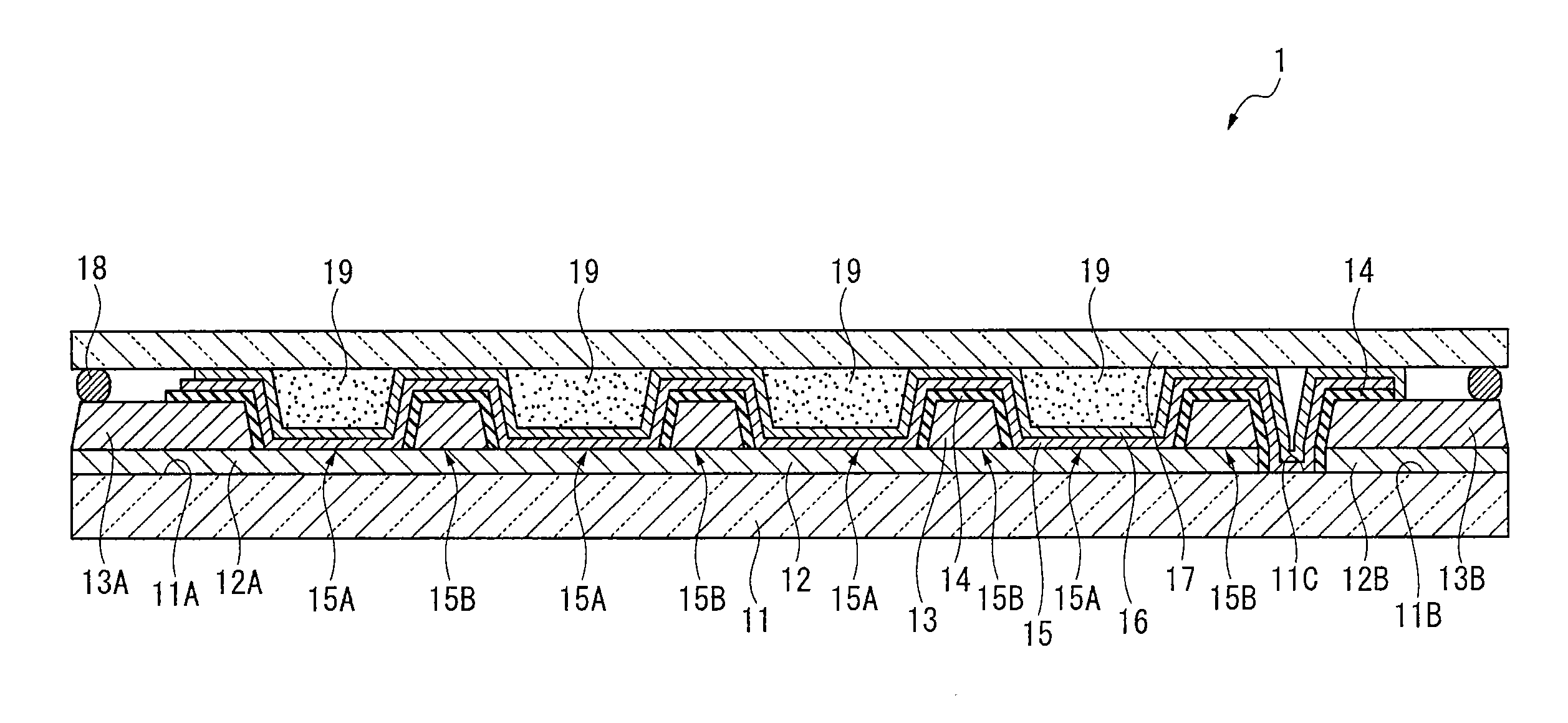
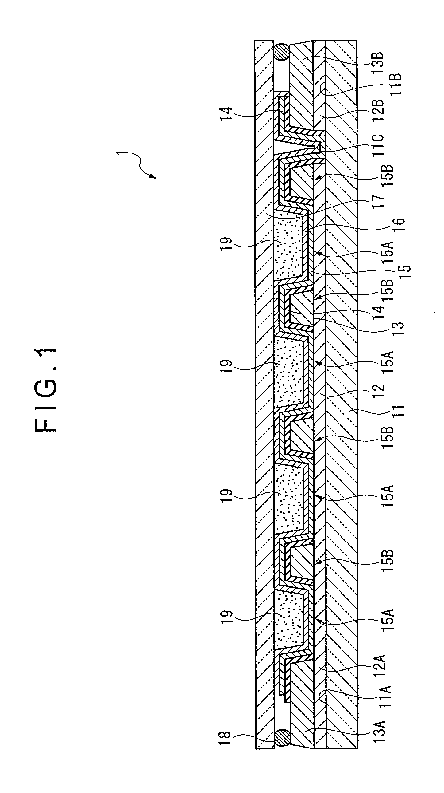
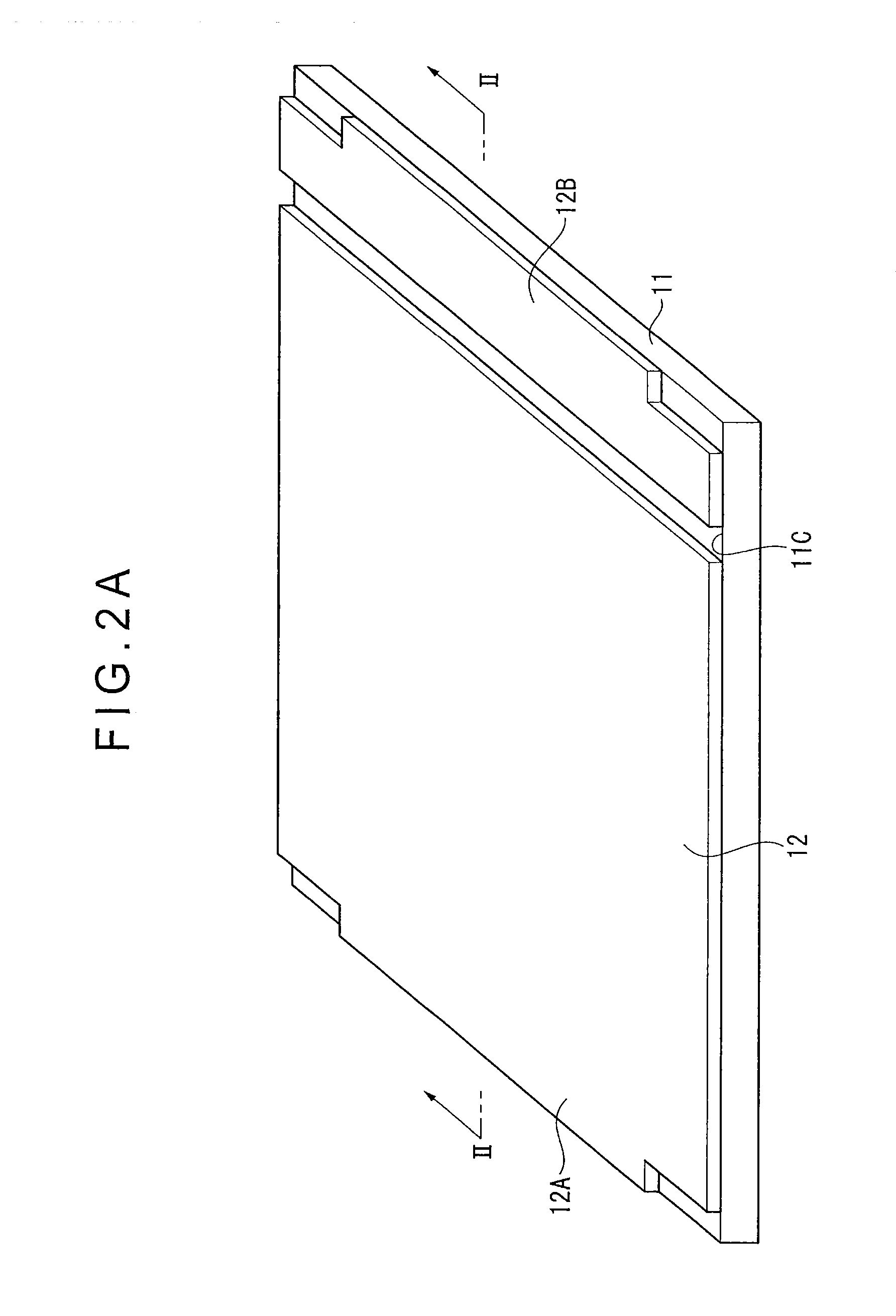
[0082]FIG. 1 is a cross section in a substrate-thickness direction showing a photoelectric conversion device 1 according to the first exemplary embodiment of the invention. FIGS. 2A to 9 are perspective views or cross sectional views showing production steps of the photoelectric conversion device 1.
[0083]The photoelectric conversion device 1 includes a first substrate 11, a first electrode 12, an organic layer 15, a second electrode 16 and a second substrate 17 arranged in this order. The first electrode 12, the organic layer 15 and the second electrode 16 provides a photoelectric conversion element. In the first exemplary embodiment, the photoelectric conversion element in a form of an organic EL device will be described. An auxiliary electrode 13 is disposed between the first electrode 12 and the organic layer 15. A...
second exemplary embodiment
[0176]Next, a second exemplary embodiment of the invention will be described below with reference to the attached drawings.
[0177]As shown in FIG. 10, a photoelectric conversion device 2 according to the second exemplary embodiment is similar to the photoelectric conversion device 1 according to the first exemplary embodiment except that the insulative portion is not interposed between the auxiliary electrode 13 and the organic layer 15. In the description of the second exemplary embodiment, the same components as those in the first exemplary embodiment are denoted by the same reference signs to simplify or omit an explanation of the components.
[0178]In the photoelectric conversion device 2, the organic layer 15 around the area in which the auxiliary electrode 13 is provided tends to preferentially cause light emission. Accordingly, by narrowing the intervals between the lines defining the frame of the auxiliary electrode 13, the luminous areas can be made closer to each other, so th...
third exemplary embodiment
[0181]Next, a third exemplary embodiment of the invention will be described below with reference to the attached drawings.
[0182]As shown in FIG. 11, a photoelectric conversion device according to the third exemplary embodiment is similar to the photoelectric conversion device 1 according to the first exemplary embodiment except that the shape of the auxiliary electrode 13 is different from that of the auxiliary electrode 13 in the first exemplary embodiment. In the description of the third exemplary embodiment, the same components as those in the first exemplary embodiment are denoted by the same reference signs to simplify or omit an explanation of the components.
[0183]In the photoelectric conversion device according to the third exemplary embodiment, the auxiliary electrode pattern provided by an auxiliary electrode 33 is not in the frame shape as in the auxiliary electrode 13 according to the first exemplary embodiment but is in the shape of an end of a fork. Specifically, a plur...
PUM
 Abstract
Description
Claims
Application Information