CMOS Image Sensors Implementing Full Frame Digital Correlated Double Sampling with Global Shutter

a cmos image sensor and global shutter technology, applied in the field of active pixel cmos image sensor, can solve the problems of higher power, geometric distortion, and more expensive compared to typical cmos sensor

Inactive Publication Date: 2013-10-03
PIXIM
View PDF3 Cites 28 Cited by
  • Summary
  • Abstract
  • Description
  • Claims
  • Application Information

AI Technical Summary

Benefits of technology

[0009]According to one embodiment of the present invention, an image sensing device includes a two-dimensional array of light sensing elements where each light sensing element includes a photodiode and multiple control transistors. Each photodiode generates an output signal indicative of an intensity level of light impinging on the photodiode and the control transistors are configured to control reset, charge transfer and row select operations of the array of light sensing elements. The image sensing device further includes a timing and control circuit configured to generate control signals for the control transistors in each light sensing element in the array where the control signals controlling reset, light integration, charge transfer and readout operations of the array of light sensing elements; one or more analog-to-digital converters coupled to columns of the array of light sensing elements and configured to digitize output signals read out from

Problems solved by technology

CCD image sensors are not preferred in modern designs in part because CCDs typically consume a higher level of power, and require a relatively complex analog front end circuit.
As a result, rolling shutter causes geometric

Method used


Image

  • CMOS Image Sensors Implementing Full Frame Digital Correlated Double Sampling with Global Shutter
  • CMOS Image Sensors Implementing Full Frame Digital Correlated Double Sampling with Global Shutter
  • CMOS Image Sensors Implementing Full Frame Digital Correlated Double Sampling with Global Shutter

Examples


Embodiment Construction

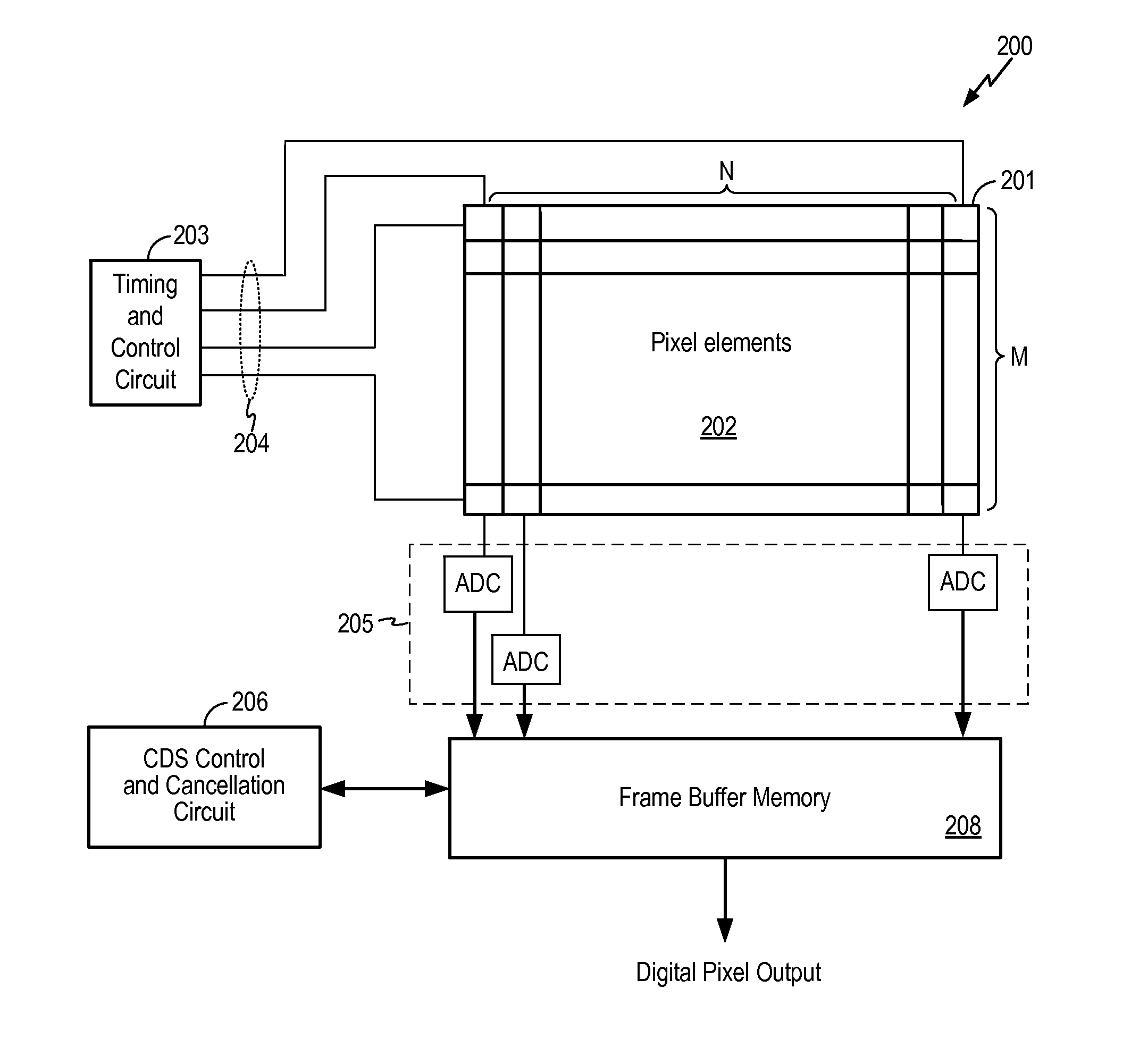
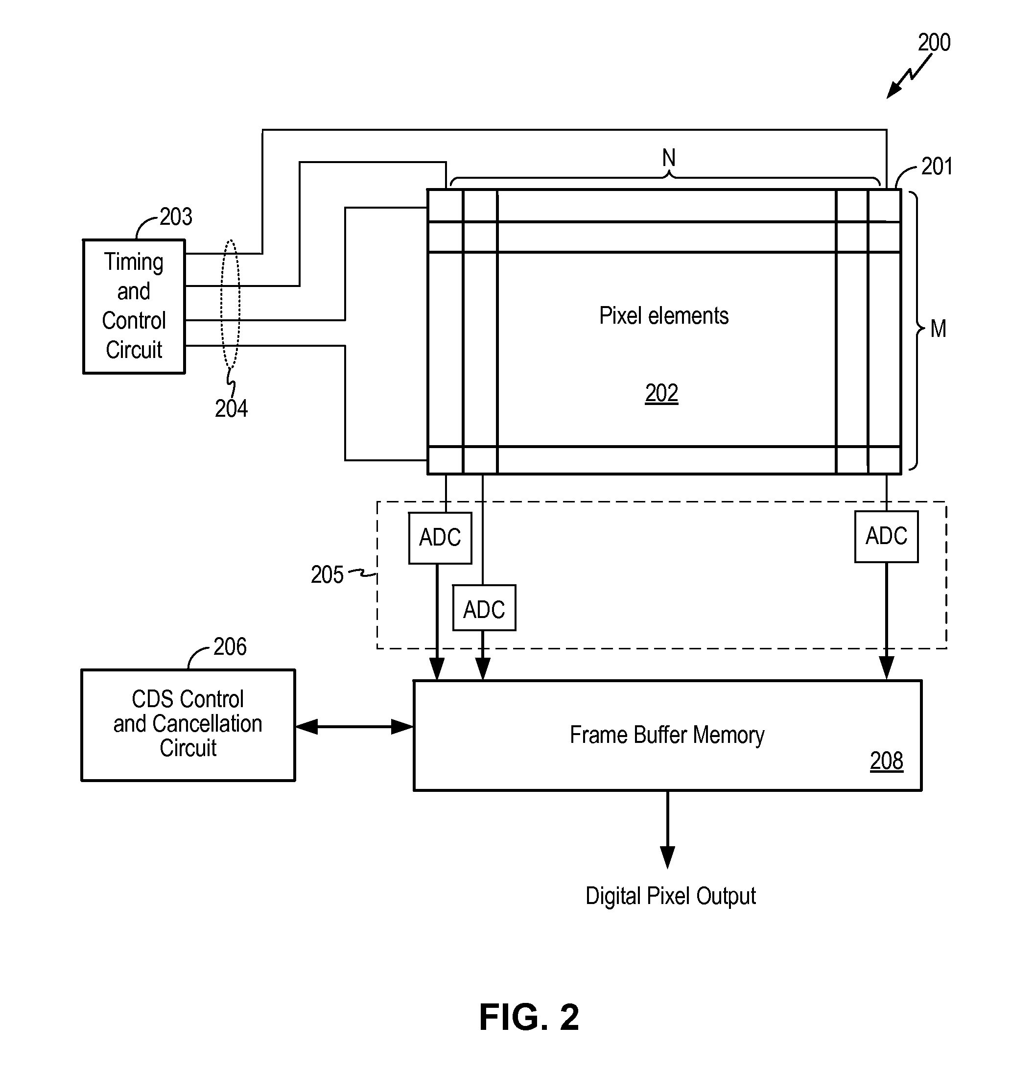
[0021]In accordance with the principles of the present invention, an active pixel CMOS image sensor implements full frame digital correlated double sampling (CDS) with global shutter. To implement full frame digital correlated double sampling with global shutter, all the pixels in the image sensor are reset at substantially the same time and all the pixels in the image sensor integrate incident light at substantially the same time and for substantially the same time duration and correlated double sampling cancellation is performed in the digital domain. In one embodiment, the image sensor includes an array of pixel elements and a timing and control logic circuit. The timing and control logic circuit in the image sensor controls the reset, the beginning and the end of exposure or light integration for all pixel elements so that the reset period and exposure period occur at substantially the same time and for substantially the same duration for all the pixels. The pixel reset values o...


PUM


Abstract

An active pixel CMOS image sensor implements full frame digital correlated double sampling (CDS) with global shutter where all the pixels in the image sensor are reset at substantially the same time and all the pixels in the image sensor integrate incident light at substantially the same time and for substantially the same time duration and correlated double sampling cancellation is performed in the digital domain. In one embodiment, the image sensing device includes an array of light sensing elements, a timing and control circuit and analog-to-digital converters. The timing and control circuit is operative to reset the light sensing elements in the array and to control the array of light sensing elements to integrate incident light. The pixel reset values are cancelled from the corresponding light dependent pixel values for each of the light sensing elements to generate correlated double sampling (CDS) corrected digital output pixel values.

Description

FIELD OF THE INVENTION[0001]The invention relates to image sensor systems and, in particular, to active pixel CMOS image sensors implementing full frame digital correlated double sampling with global shutter.DESCRIPTION OF THE RELATED ART[0002]Digital image capturing devices use image sensors to convert incident light energy into electrical signals. An area image sensor includes a two-dimensional array of light sensing elements called pixels. Each pixel in the array works with the lens system to respond to incident light within a local area of the scene, and produces an electrical signal describing the local characteristics of the scene. Outputs from the light sensing elements are converted to digital form and stored digitally to form the raw data representing the scene. The raw data can be processed by an image processor to produce rendered digital images.[0003]Image sensor designs include Charged Coupled Devices (CCD), Complementary Metal Oxide Silicon (CMOS) image sensors, and Di...

Claims


Application Information

Patent Timeline
IPC IPC(8): H04N5/335
CPCH04N5/378H04N5/3575H04N25/57H04N25/616H04N25/622H04N25/75
Inventor AYERS, THOMASBRADY, FREDERICK THOMASKANG, JINSUKWONG, PING WAH
Owner PIXIM
Why Eureka
Try Eureka