Pixel structure for electrowetting display devices and method of manufacturing the same
- Summary
- Abstract
- Description
- Claims
- Application Information
AI Technical Summary
Benefits of technology
Problems solved by technology
Method used
Image

Examples
Embodiment Construction
[0035]Hereinafter, exemplary embodiments of the present invention will be described with reference to the accompanying drawings in detail.
[0036]It will be understood that when an element or layer is referred to as being “on”, “connected to” or “coupled to” another element or layer, it can be directly on, connected or coupled to the other element or layer or intervening elements or layers may be present.
[0037]As used herein, the singular forms, “a”, “an” and “the” are intended to include the plural forms as well, unless the context clearly indicates otherwise. As used herein, the term “and / or” includes any and all combinations of one or more of the associated listed items.
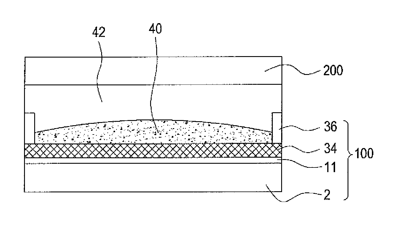
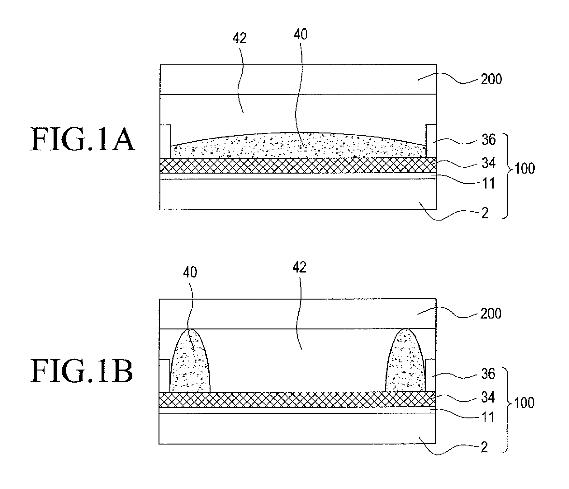
[0038]FIGS. 1A and 1B are magnified sectional views of a schematic pixel of an electrowetting display device. The electrowetting display device includes a first display substrate 100, a hydrophobic fluid 40 positioned on the first display substrate 100, a hydrophilic fluid 42 positioned on the hydrophobic fluid 40 w...
PUM
 Abstract
Description
Claims
Application Information
 - R&D
- Intellectual Property
- Life Sciences
- Materials
- Tech Scout
- Unparalleled Data Quality
- Higher Quality Content
- 60% Fewer Hallucinations
Browse by: Latest US Patents, China's latest patents, Technical Efficacy Thesaurus, Application Domain, Technology Topic, Popular Technical Reports.
© 2025 PatSnap. All rights reserved.Legal|Privacy policy|Modern Slavery Act Transparency Statement|Sitemap|About US| Contact US: help@patsnap.com