Method for Keyhole Repair in Replacement Metal Gate Integration Through the Use of a Printable Dielectric

a technology of dielectric and keyhole, applied in the field of field-effect transistors, can solve the problems of unintentional shorting of adjacent devices or circuits, major keyhole formation during the dielectric deposition process,

Inactive Publication Date: 2013-10-24
ALSEPHINA INNOVATIONS INC
View PDF2 Cites 14 Cited by
  • Summary
  • Abstract
  • Description
  • Claims
  • Application Information

AI Technical Summary

Benefits of technology

[0006]The present invention provides techniques for fabricating field-effect transistor (FET) devices that implement a modified keyhole repair process. In one aspect of the invention, a method of fabricating a FET device is provided. The method includes the following steps. A wafer is provided. At least one active area is formed in the wafer. A plurality of dummy gates are formed over the active area, wherein the dummy gates cover portions of the active area that serve as channel regions of the device and wherein portions of the active area that extend out from under the dummy gates serve as source and drain regions of the device. Spaces between the dummy gates are filled with a dielectric gap ...

Problems solved by technology

The formation of keyholes during the dielectric deposition process can be a major problem in replacement metal gate processes.
Namely, unwan...

Method used


Image

  • Method for Keyhole Repair in Replacement Metal Gate Integration Through the Use of a Printable Dielectric
  • Method for Keyhole Repair in Replacement Metal Gate Integration Through the Use of a Printable Dielectric
  • Method for Keyhole Repair in Replacement Metal Gate Integration Through the Use of a Printable Dielectric

Examples


Embodiment Construction

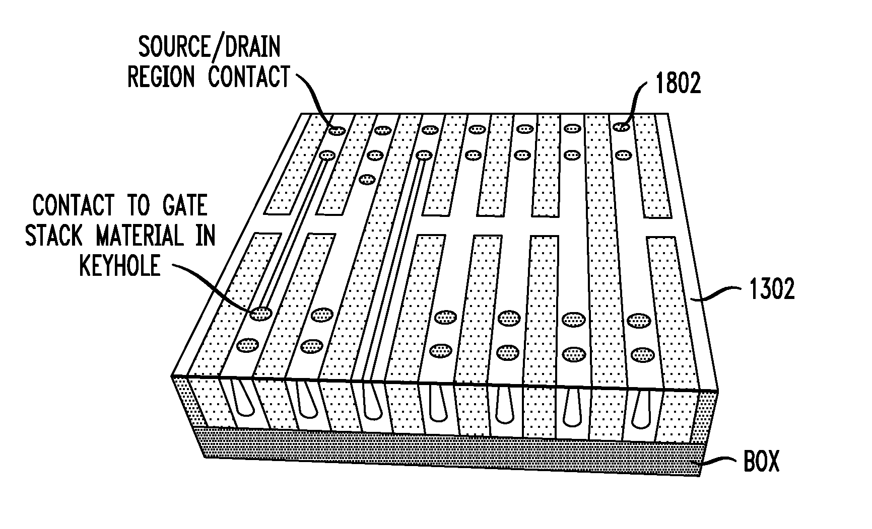
[0037]The present teachings address the notion that in certain situations the formation of keyholes during dielectric deposition is advantageous / desirable, while in other situations it is not. The present teachings take advantage of the fact that keyhole formation is highly reproducible and can be controlled through the geometry of the structures present on the wafer at the time of film deposition and the parameters of the film deposition process. Therefore, as presented herein, the benefits of keyhole formation can be selectively exploited (for instance in the formation of interconnect structures used to propagate an electrical signal, see below) exclusive of any undesired effects (formation of parasitic metal “stringers”).

[0038]The present techniques are generally applicable to any transistor or memory device fabrication process wherein dummy structures (such as dummy gates) are employed, wherein keyholes are intentionally formed during deposition of a dielectric around the dummy ...


PUM


Abstract

A method of fabricating a FET device is provided that includes the following steps. A wafer is provided. At least one active area is formed in the wafer. A plurality of dummy gates is formed over the active area. Spaces between the dummy gates are filled with a dielectric gap fill material such that one or more keyholes are formed in the dielectric gap fill material between the dummy gates. The dummy gates are removed to reveal a plurality of gate canyons in the dielectric gap fill material. A mask is formed that divides at least one of the gate canyons, blocks off one or more of the keyholes and leaves one or more of the keyholes un-blocked. At least one gate stack material is deposited onto the wafer filling the gate canyons and the un-blocked keyholes. A FET device is also provided.

Description

FIELD OF THE INVENTION[0001]The present invention relates to field-effect transistor (FET) devices, and more particularly, to techniques for fabricating FET devices that implement a modified keyhole repair process that permits use of keyholes, where desired.BACKGROUND OF THE INVENTION[0002]Replacement metal gate transistor processing relies on the encapsulation of a dummy gate material in a dielectric fill. See, for example, U.S. Pat. No. 7,923,337, issued to Chang et al., entitled “Fin Field Effect Transistor Devices with Self-Aligned Source and Drain Regions,” the entire contents of which are incorporated by reference herein.[0003]The dielectric fill serves both a structural and electrical purpose. Specifically, the dielectric fill allows for the selective removal of the dummy gate material. The dielectric fill is also used to insulate between the source / drain (S / D) contact and the gate electrode.[0004]When the dielectric material is deposited around the dummy gates, keyholes, air...

Claims


Application Information

Patent Timeline
IPC IPC(8): H01L27/088H01L21/8234
CPCH01L21/823828H01L27/0207H01L21/28017H01L29/66545H01L21/02134H01L21/0274H01L21/823431H01L21/823437H01L21/845H01L29/16
Inventor CHANG, JOSEPHINE B.GUILLORN, MICHAEL A.SLEIGHT, JEFFREY W.
Owner ALSEPHINA INNOVATIONS INC
Why Eureka
Try Eureka