Copper interconnect with CVD liner and metallic cap

Active Publication Date: 2013-10-24
IBM CORP +3
View PDF8 Cites 25 Cited by
  • Summary
  • Abstract
  • Description
  • Claims
  • Application Information

AI Technical Summary

Benefits of technology

The patent describes a structure and method for depositing a diffusion barrier within an opening in a layer of dielectric material. The structure includes a metal liner, a seed layer, copper material, a metallic cap, and a capping layer. The technique involves depositing the metal liner on top of the diffusion barrier, adding the copper seed layer on top of the metal liner, filling the opening with copper material, depositing the metallic cap selective to copper material, and adding the capping layer on top of the metallic cap. This approach provides a better barrier against copper diffusion and improved reliability during semiconductor device fabrication.

Problems solved by technology

Poor or inadequate copper seed layer coverage results in poor electroplating of the copper and poor electromigration characteristics.

Method used


Image

  • Copper interconnect with CVD liner and metallic cap
  • Copper interconnect with CVD liner and metallic cap
  • Copper interconnect with CVD liner and metallic cap

Examples


Embodiment Construction

[0014]Detailed embodiments of the claimed structures and methods are disclosed herein; however, it is understood that the disclosed embodiments are merely illustrative of the claimed structures and methods that may be embodied in various forms. This disclosure may, however, be embodied in many different forms and should not be construed as limited to the exemplary embodiment set forth herein. Rather, these exemplary embodiments are provided so that this disclosure will be thorough and complete and will fully convey the scope of this disclosure to those skilled in the art. In the description, details of well-known features and techniques may be omitted to avoid unnecessarily obscuring the presented embodiments.

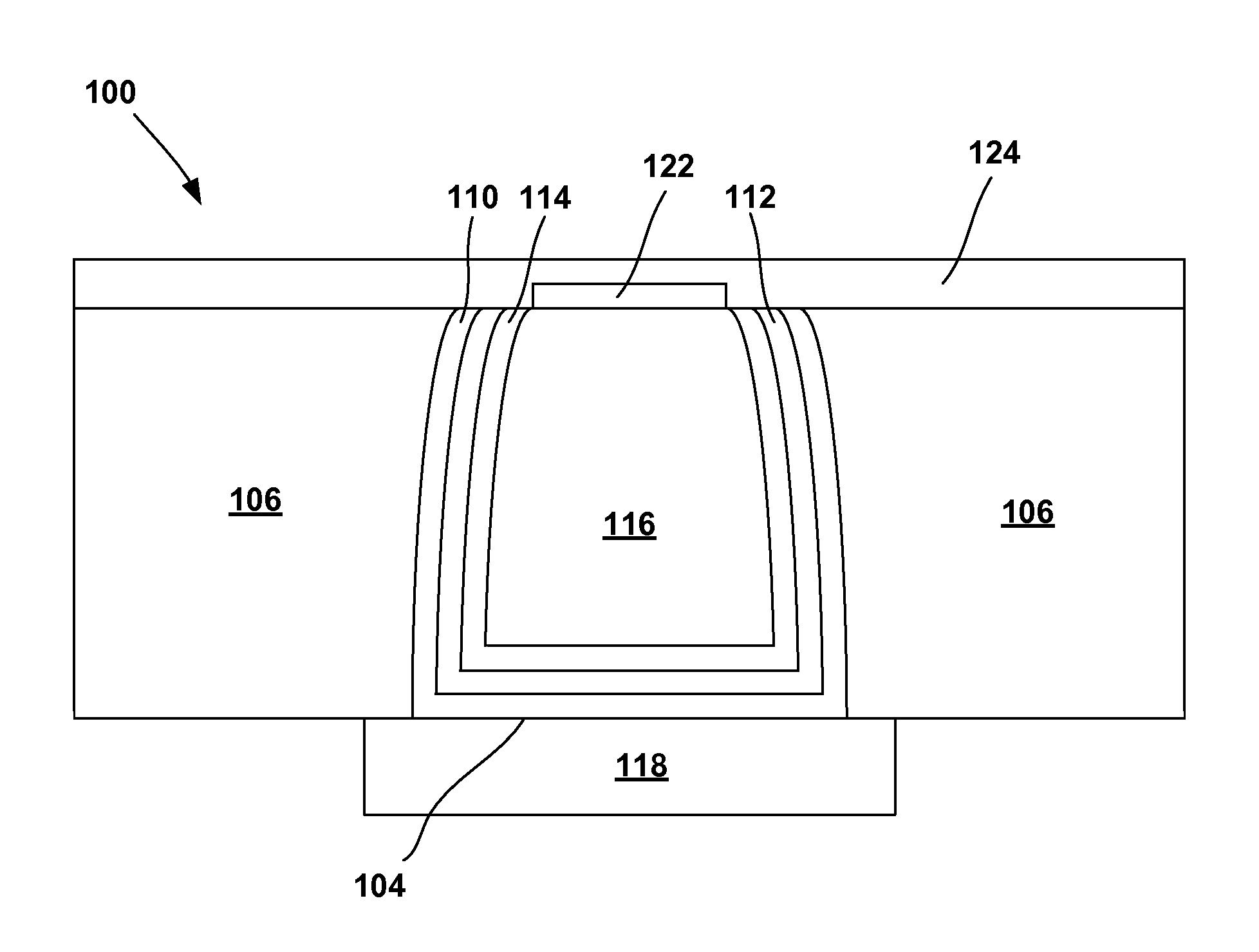
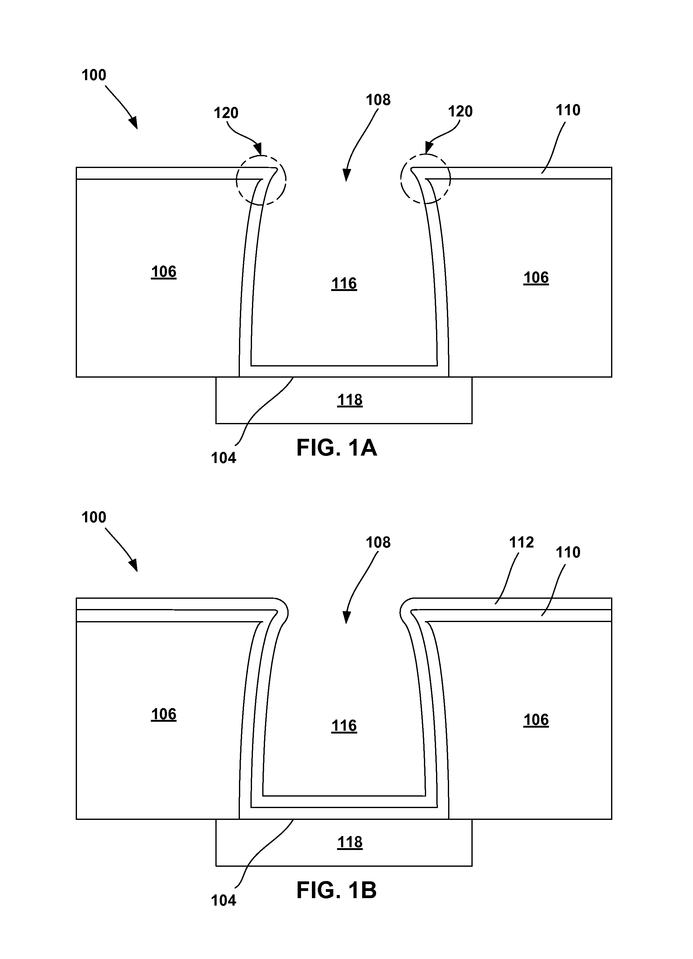
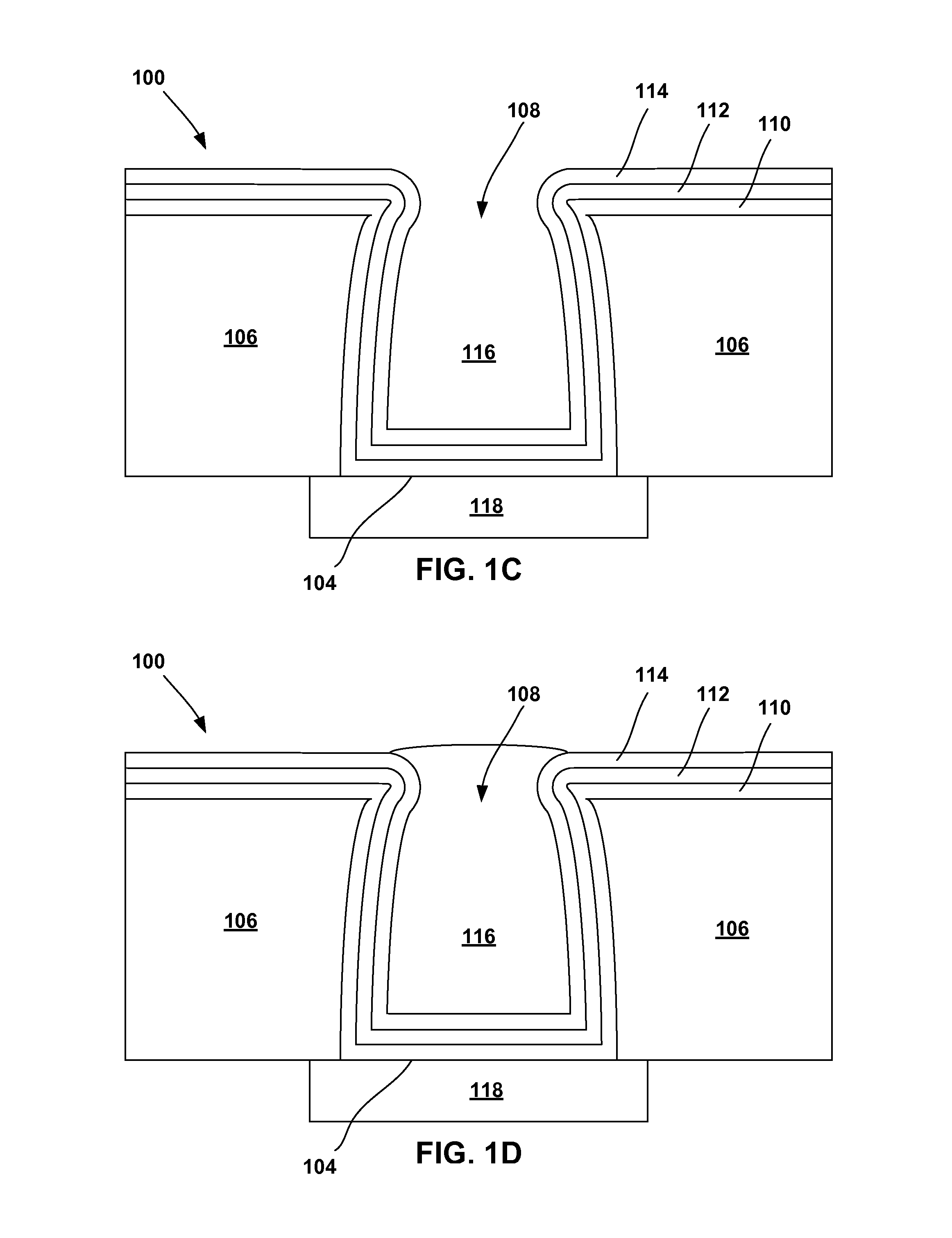
[0015]FIG. 1A illustrates a cross-sectional view of a step of a method in forming a copper interconnect 100. The step includes creating an opening 108 in a layer of dielectric material 106, which exposes a copper pad 118 positioned at a bottom 104 of the opening 108. The copper...


PUM


Abstract

A structure having a diffusion barrier positioned adjacent to a sidewall and a bottom of an opening being etched in a layer of dielectric material. The structure also having a metal liner positioned directly on top of the diffusion barrier, a seed layer positioned directly on top of the metal liner, wherein the seed layer is made from a material comprising copper, a copper material positioned directly on top of the seed layer, a metallic cap positioned directly on top of and selective to the copper material, and a capping layer positioned directly on top of and adjacent to the metallic cap.

Description

FIELD OF THE INVENTION[0001]The present invention generally relates to integrated circuits, and particularly to copper interconnect structures.BACKGROUND OF INVENTION[0002]Copper interconnects provide the primary connectivity and / or electrical pathway within a semiconductor device. Copper may be the primary element used to form such interconnects because of its electrical conductive properties. Copper interconnects can be formed within an opening or multiple openings etched in a layer of dielectric material. These openings commonly take the shape of wires, trenches, or vias. A diffusion barrier may be used to prevent diffusion of copper into the surrounding dielectric material. A copper seed layer can be deposited prior to filling the opening with copper using an electroplating technique. The opening(s) etched in the layer of dielectric can have re-entrant features which can prevent adequate deposition of the copper seed layer. Poor or inadequate copper seed layer coverage results i...

Claims


Application Information

Patent Timeline
IPC IPC(8): H01L23/532H01L21/768
CPCH01L21/76804H01L21/76843H01L21/76849H01L21/76873H01L23/53238H01L2924/0002H01L2924/00
Inventor BAUMANN, FRIEDER HAINRICHHU, CHAO-KUNSIMON, ANDREW H.BOLOM, TIBORMOTOYAMA, KOICHINIU, CHENGYU CHARLES
Owner IBM CORP
Why Eureka
Try Eureka